Solid electrolytic capacitor and method for manufacturing the same
a solid electrolytic capacitor and capacitor technology, applied in the field can solve the problems of difficult formation of solid electrolyte layers having an uniform thickness on the surface of dielectric coatings, and achieve the effects of suppressing electrical short circuit between the anode body and the cathode layer, increasing the reliability and reducing the number of solid electrolytic capacitors
- Summary
- Abstract
- Description
- Claims
- Application Information
AI Technical Summary
Benefits of technology
Problems solved by technology
Method used
Image
Examples
first embodiment
[0021
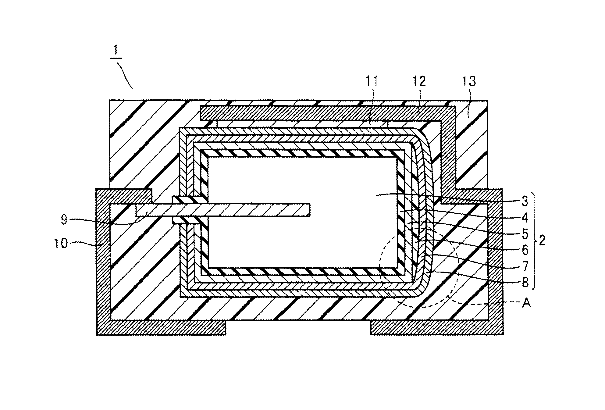
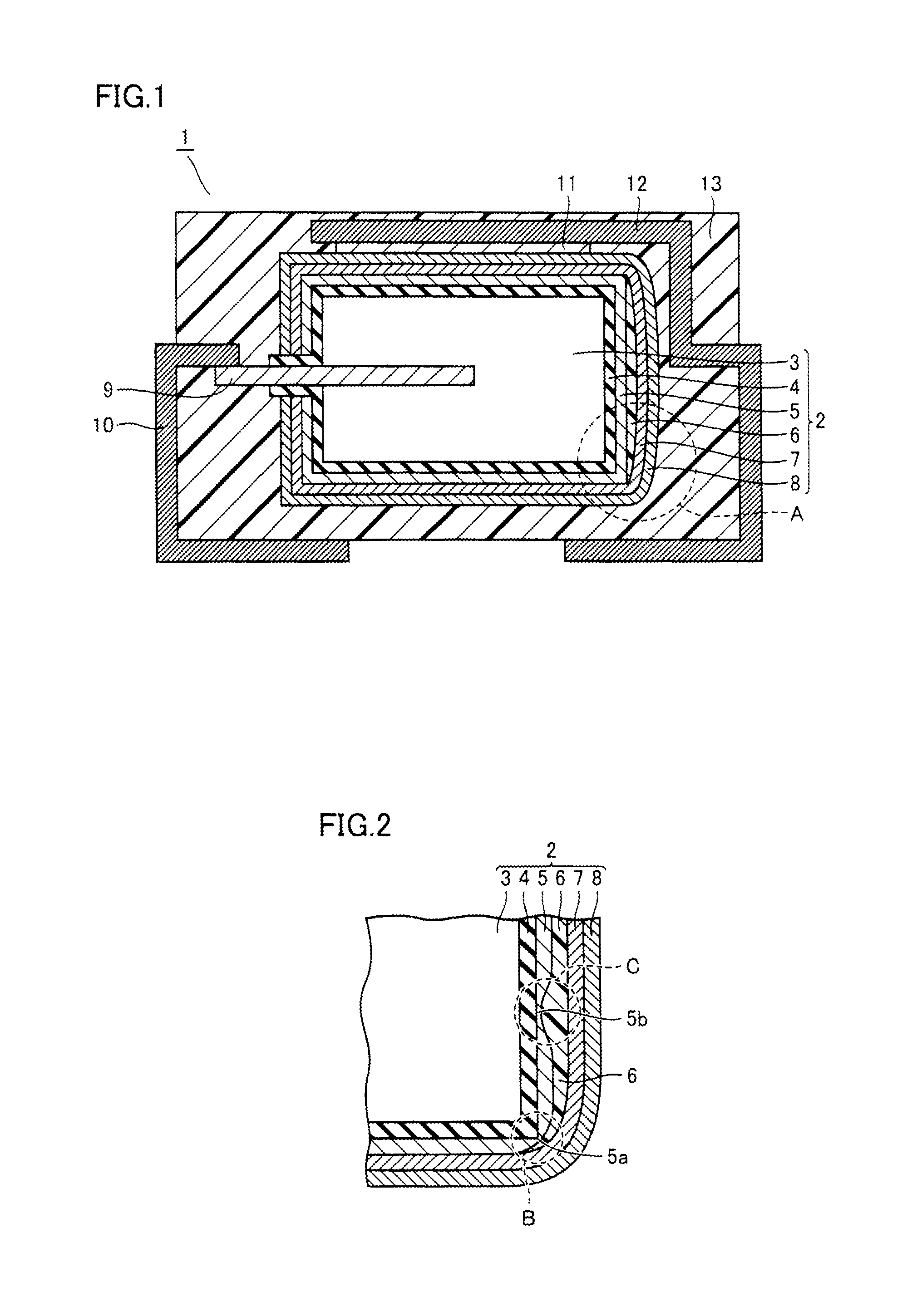
[0022]A description will be given to a solid electrolytic capacitor according to a first embodiment of the present invention. As shown in FIG. 1, a capacitor element 2 serving as a capacitor main body in a solid electrolytic capacitor 1 includes an anode body 3 serving as an anode, a dielectric coating 4, a solid electrolyte layer 5, an insulating layer 6, and a carbon layer 7 and a silver paste layer 8 serving as a cathode.
[0023]Anode body 3 of capacitor element 2 has an anode lead 9 provided in an upright manner and one end of an anode terminal 10 is electrically connected to anode lead 9. One end side of a cathode terminal 12 is electrically connected to silver paste layer 8 of capacitor element 2 with a conductive bonding layer 11 interposed therebetween. An exterior resin 13 seals capacitor element 2 in such a manner that the other end side of anode terminal 10 and the other end side of cathode terminal 12 are exposed.
[0024]Next, a structure of capacitor element 2 will be ...
second embodiment
[0029
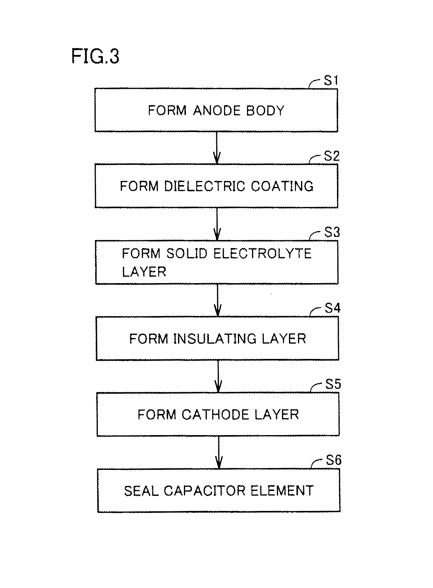
[0030]A description will be given to one example of a method for manufacturing the above-mentioned solid electrolytic capacitor as a second embodiment of the present invention. FIG. 3 shows one example of a manufacturing flow. As shown in FIGS. 3 and 1, an anode body is first formed in step S1. Metal powder having the valve action is prepared, and this metal powder is molded into a desired shape, with one end side of anode lead 9 in the longitudinal direction buried into the metal powder. Next, the molded body is sintered to form anode body 3. This anode body 3 may be porous.
[0031]Next, a dielectric coating is formed in step S2. Anode body 3 is subjected to chemical conversion treatment, and thereby dielectric coating 4 is formed to cover anode body 3. As the chemical conversion treatment, there is a method for soaking anode body 3 in a chemical conversion solution such as a phosphoric acid aqueous solution or nitric acid aqueous solution, and applying a predetermined voltage, ...
PUM
| Property | Measurement | Unit |
|---|---|---|
| insulating | aaaaa | aaaaa |
| size | aaaaa | aaaaa |
| conductive | aaaaa | aaaaa |
Abstract
Description
Claims
Application Information


