

Substrate processing apparatus and method of manufacturing semiconductor device
a processing apparatus and semiconductor technology, applied in the direction of crystal growth process, polycrystalline material growth, transportation and packaging, etc., can solve the problems of the temperature of the furnace port of each member may not be able to remain below, and the heat deterioration of the member to achieve the effect of suppressing heat deterioration
- Summary
- Abstract
- Description
- Claims
- Application Information
AI Technical Summary
Benefits of technology
Problems solved by technology
Method used
Image

Examples
first embodiment
[0082
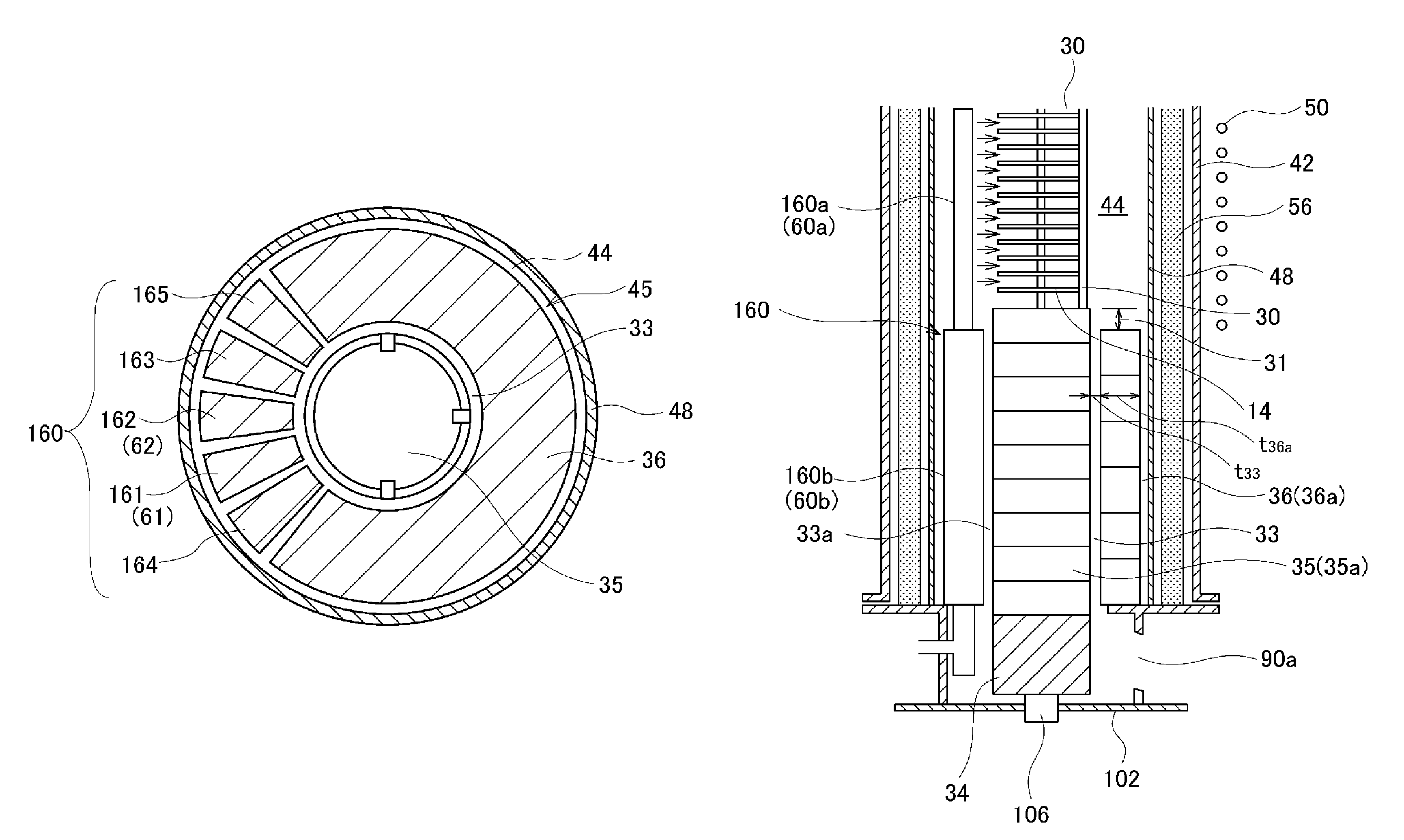
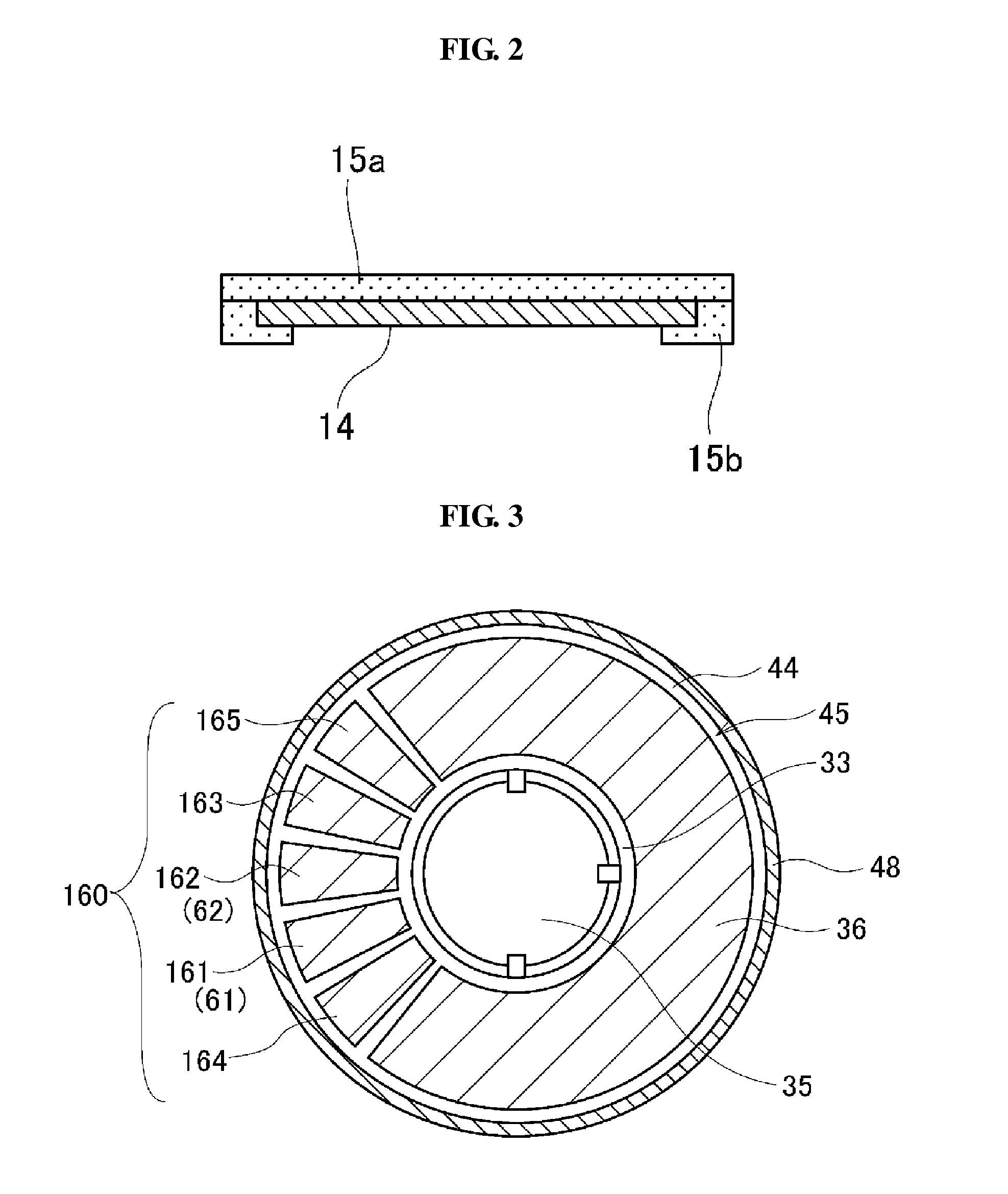
[0083]In FIG. 6, a schematic view of the lower structure of the processing furnace according to a first embodiment is shown, and in FIG. 13, a detailed perspective cross-sectional view of the lower structure is shown. In addition, in FIG. 6, a wafer holder 15 is omitted, and the wafer 14 is used instead of the wafer holder.
Hollow Heat Exchange Unit
[0084]As shown in FIG. 6, the first heat exchange unit 35 and the heat insulating cylinder 34 are disposed on the lower side of the boat 30. The first heat exchange unit 35 includes a heat exchange unit formed in a hollow cylindrical shape, for example a center heat insulating cylinder 35a composed of a heat insulating member. In the horizontal direction of the center heat insulating cylinder 35a, the second heat exchange unit 36 is disposed to form the gap 33 with the center heat insulating cylinder 35a. The second heat exchange unit 36 includes a heat exchange unit formed in a hollow cylindrical shape, for example, a peripheral edge...
second embodiment
[0130
[0131]In FIGS. 16 and 17, a second embodiment in which the heat exchanger constituting the first and second heat exchange units is configured as a heat insulating plate is shown. That is, instead of the heat exchange unit formed in the hollow cylindrical shape or the stacked heat exchangers, a plurality of heat insulating plates 59 are provided. As the heat insulating plate 59, a heat insulating plate 59a formed in a disc shape is used in the first heat exchange unit, and a heat insulating plate 59b formed in a ring plate shape is used in the second heat exchange unit. In order to cut off radiation of a high temperature from the wafer region 43, the heat insulating plate 59 is preferably used because effects become higher as the number of the heat insulating plates 59 is increased. However, when a process gas with a large flow rate is required, heat that is transmitted to the outside of the furnace by the gas as well as radiation should be considered. Heat exchange is required ...
third embodiment
[0132
[0133]In FIG. 18, a processing furnace of the third embodiment in which the substrate heating unit is configured as a resistance heating body instead of an induction heating body composed of the above-described induction coil and the object to be heated is shown.
[0134]Unlike the processing furnace shown in FIG. 16, the processing furnace shown in FIG. 18 does not require an induction heating member such as the body to be heated 48, the outer heat insulating wall 56, the induction coil 50, or the like. As shown in FIG. 18, the processing furnace is formed in a reaction vessel including the reaction tube 42 made of quartz and the manifold 46, and includes the process chamber 44 for processing the wafers 14, a resistance heating heater 48a that is provided on the outer periphery of the reaction tube 42 and acts as a heating body for heating the wafer 14 in the process chamber 44, and a boat 30 that holds the plurality of wafers 14 in the process chamber 44 to have an interval with...
PUM
| Property | Measurement | Unit |
|---|---|---|
| temperature | aaaaa | aaaaa |
| temperature | aaaaa | aaaaa |
| temperature | aaaaa | aaaaa |
Abstract
Description
Claims
Application Information