Light-emitting device and method of manufacturing the same

a technology of light-emitting devices and manufacturing methods, which is applied in the direction of electroluminescent light sources, lighting and heating apparatus, electric lighting sources, etc., can solve the problems of deterioration of the sealing portion b>3/b>, and achieve the effects of reducing the thermal resistance between the phosphor particles and the conductor layer, suppressing heat deterioration in the members, and enhancing the heat dissipation of the phosphor particles

Active Publication Date: 2016-04-12
TOYODA GOSEI CO LTD
View PDF17 Cites 2 Cited by
  • Summary
  • Abstract
  • Description
  • Claims
  • Application Information

AI Technical Summary

Benefits of technology

[0037]According to one embodiment of the invention, a light-emitting device is constructed such that a phosphor layer is arranged above a light-emitting element, and a resin layer contacts both of a phosphor layer and a conductor layer and contains heat-conductive particles dispersed therein, wherein the heat-conductive particles have a thermal conductivity of not less than 100 W / m·K and an insulator property or a semiconductor property.
[0038]Thus, since the heat-conductive particles are disposed dispersed between the phosphor layer as a heat-generating body and the conductor layer as a heat-dissipating route, the thermal resistance between the phosphor particles and the conductor layer can be reduced so as to enhance the heat dissipation from the phosphor particles. Thereby, it is possible to suppress heat deterioration in members composing the light-emitting device.
[0039]Light-diffusing particles for diffusing light, such as SiO2, TiO2 and Al2O3 are generally contained as a filler in a sealing portion but the thermal conductivities of SiO2, TiO2 and Al2O3 are only about 1.5 W / m·K, 10 W / m·K and 30 W / m·K, respectively, and therefore, an effect of improving a thermal conductivity is insufficient.
[0040]The invention focuses on improvement in thermal conductivity, not on improvement in light-diffusing properties. Therefore, the configuration and effect of the filler are different from the conventional filler contained in a sealing portion. And also, a positional relation between phosphor particles and the filler and an effect resulting therefrom are also different.
[0041]In addition, “a conductor layer connected to an external power source” in the embodiment of the invention includes an external electrical connection lead of the LED lamp and a wiring or metal substrate of the COB module and it is acceptable as long as it is a conductor electrically or thermally connected to the external power source.

Problems solved by technology

Therefore, the separate arrangement has a problem that the heat generated by the phosphor particles 3a is not sufficiently dissipated and deterioration of the sealing portion 3 is thus likely to occur.

Method used


Image

  • Light-emitting device and method of manufacturing the same
  • Light-emitting device and method of manufacturing the same
  • Light-emitting device and method of manufacturing the same

Examples


first embodiment

[0048]the invention will be described below in reference to the appended drawings.

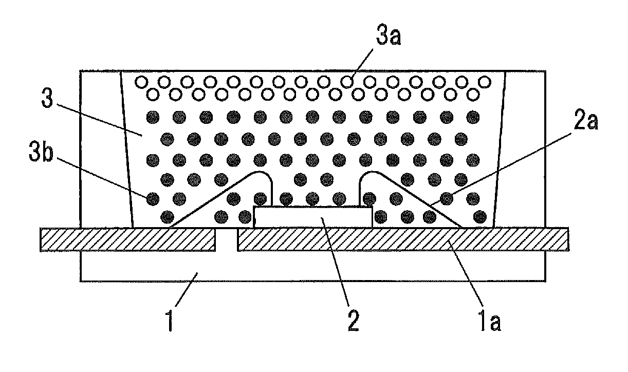
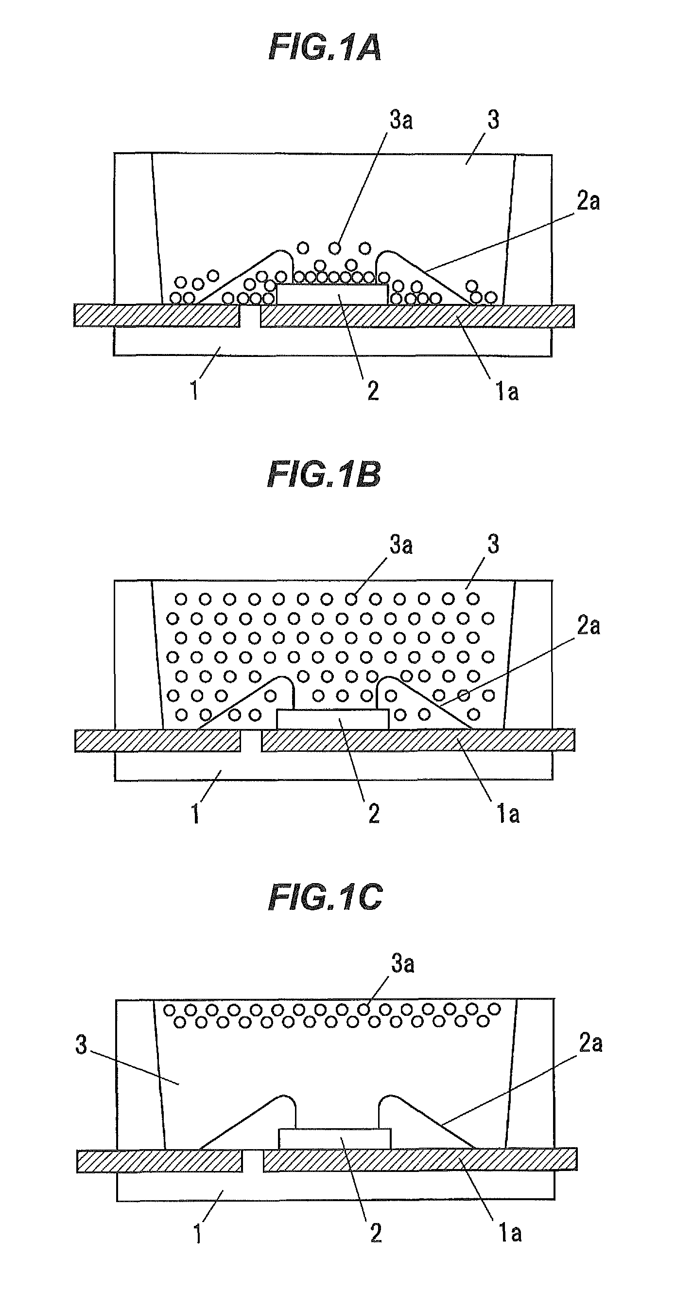
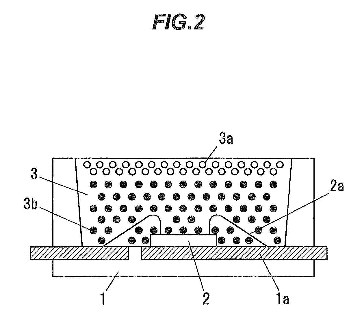
[0049]FIG. 2 is a cross sectional view showing an LED lamp in the first embodiment of the invention.

[0050]The LED lamp in the first embodiment of the invention is composed of a package 1 having a pair of leads 1a on a bottom surface of a recessed portion, an LED chip 2 which is formed of an inorganic compound semiconductor emitting ultraviolet to blue light and is mounted on one of the pair of leads 1a, and a sealing portion 3 filling the recessed portion of the package 1 while being in contact with and sealing the LED chip 2.

[0051]The LED chip 2 is mounted in so-called face-up manner, and positive and negative electrodes thereof (not shown) are respectively electrically connected to the pair of leads 1a via wires 2a formed of Au, etc. The pair of leads 1a protrude outward from side surfaces of the package 1 and the protruding portions thereof function as external connection terminals. The pair of lead...

second embodiment

[0079]FIG. 3 is a cross sectional view showing an LED lamp in the invention.

[0080]The second embodiment is different from the first embodiment in that heat-conductive particles 1b are not contained in the sealing portion 3 unlike the first embodiment but are dispersed and contained in the package 1 and also a white resin portion 4 is formed so as not to overlap with a portion of the sealing portion 3 having a high concentration of the phosphor particles 3a.

[0081]The white resin portion 4 contains white pigment particles of TiO2, etc., and is formed so that a reflectivity with respect to light emitted from the LED chip 2 is higher than the package 1 which contains the heat-conductive particles 1b.

[0082]For forming the white resin portion 4 in the second embodiment, for example, the package 1 is formed by molding such as injection molding or transfer molding, and then, a thermosetting resin, such as uncured epoxy resin or silicone resin, containing white pigment particles of TiO2, e...

third embodiment

[0094]FIG. 5 is a cross sectional view showing an LED lamp in the invention.

[0095]The third embodiment is different from the first and second embodiments in that so-called flip-chip mounting in which the LED chip 2 is joined to the package at an electrode forming surface and is electrically connected to the lead 1a via bumps 2b formed of Au, etc., is employed instead of employing the so-called face-up mounting in which LED chip 2 is joined to the package at a surface opposite to the electrode forming surface and is electrically connected to the lead via the wires, and also in that the sealing portion 3 is not formed.

[0096]In other words, the LED chip 2 is sealed so that the white resin portion 4 and the plate material 5 are in contact with the LED chip 2.

[0097]For forming the white resin portion 4 in the third embodiment, for example, the package 1 is formed by molding such as injection molding or transfer molding, the LED chip 2 is subsequently flip-chip mounted via the bumps 2b, a...


PUM


Abstract

A light-emitting device includes a base material having a conductor layer on a surface thereof, the conductor layer being configured to be connected to an external power source, a light-emitting element mounted on the base, a phosphor layer arranged above the light-emitting element, and a resin layer contacting both of the phosphor layer and the conductor layer and containing heat-conductive particles dispersed therein. The heat-conductive particles have a thermal conductivity of not less than 100 W / m·K and an insulator property or a semiconductor property.

Description

[0001]The present application is based on Japanese patent application Nos. 2012-163507 and 2013-031811 filed on Jul. 24, 2012 and Feb. 21, 2013, respectively, the entire contents of which are incorporated herein by reference.BACKGROUND OF THE INVENTION[0002]1. Field of the Invention[0003]The invention relates to a light-emitting device in which a phosphor and a light-emitting element are used and a method of manufacturing the same, and in more particular, to a light-emitting device in which a phosphor and a light-emitting element are used to produce white light and a method of manufacturing the same.[0004]2. Related Art[0005]In so-called COB (Chip-on-Board) modules, plural light-emitting elements such as LED chips are mounted on a general-purpose substrate such as ceramic substrate or metal substrate. In LED lamps, a light-emitting element is mounted on a resin or ceramic package. In light-emitting devices such as COB modules or LED lamps, an LED chip emitting ultraviolet to blue li...

Claims


Application Information

Patent Timeline
Patent Type & Authority Patents(United States)
IPC IPC(8): F21V29/00H05B33/04H01L33/64H05B33/10H01L33/50
CPCH01L33/644H05B33/04H05B33/10H01L33/502H01L2224/48091H01L2224/48247H01L2924/1301
Inventor TSUCHIYA, YOSUKETAJIMA, HIROYUKISHIMONISHI, SHOTASENGOKU, AKIRA
Owner TOYODA GOSEI CO LTD
Why Eureka
Try Eureka