Oxide electronic device and method for manufacturing the same

a technology of electronic devices and oxides, applied in semiconductor devices, digital storage, instruments, etc., can solve the problems of device driving energy consumption, and device driving energy consumption, and achieve the effect of reducing the consumption of driving energy of the devi

Inactive Publication Date: 2014-11-18
KOREA INST OF SCI & TECH
View PDF10 Cites 1 Cited by
  • Summary
  • Abstract
  • Description
  • Claims
  • Application Information

AI Technical Summary

Benefits of technology

[0022]According to the present disclosure, electric conductivity of 2DEG generated at an interface of heterogeneous oxides is controlled stably in a non-volatile mode by spontaneous polarization of a ferroelectric material. As a result, electric conductivity of 2DEG is maintained continuously without external electric energy, thereby reducing consumption of the driving energy of a device.

Problems solved by technology

However, it is expected that silicon materials reach the limit in downsizing and functional upgrading within the next 10 years.
However, in this case, the electric conductivity of 2DEG controlled by such charge injection tends to have volatility with time, and thus is not maintained stably but experiences a change.
In this context, there is a problem in that continuous application of electric energy is required to prevent such volatility.
As a result, the resultant device requires a large amount of driving energy.

Method used


Image

  • Oxide electronic device and method for manufacturing the same
  • Oxide electronic device and method for manufacturing the same
  • Oxide electronic device and method for manufacturing the same

Examples


Embodiment Construction

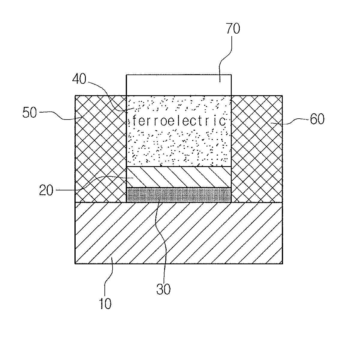
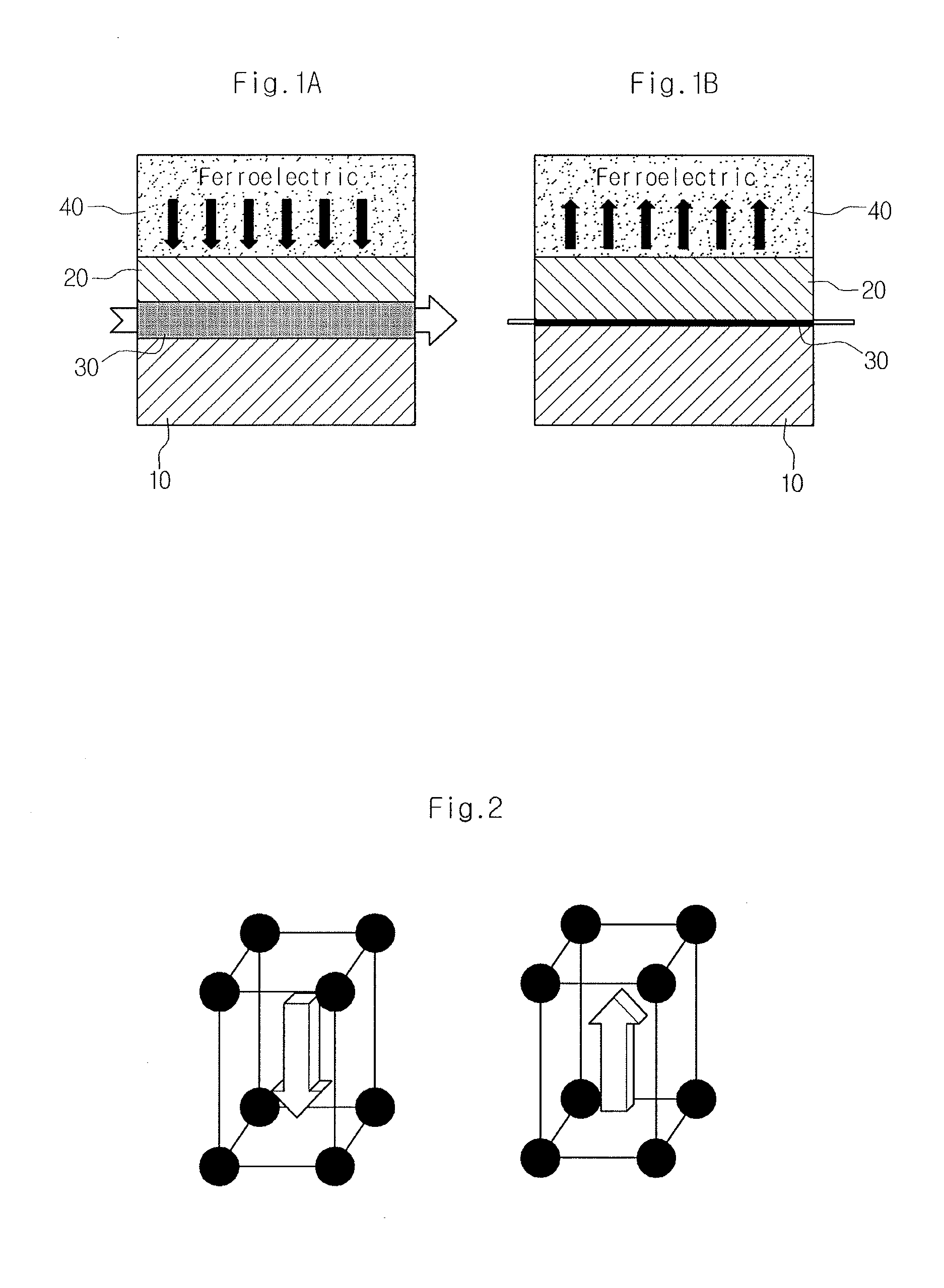
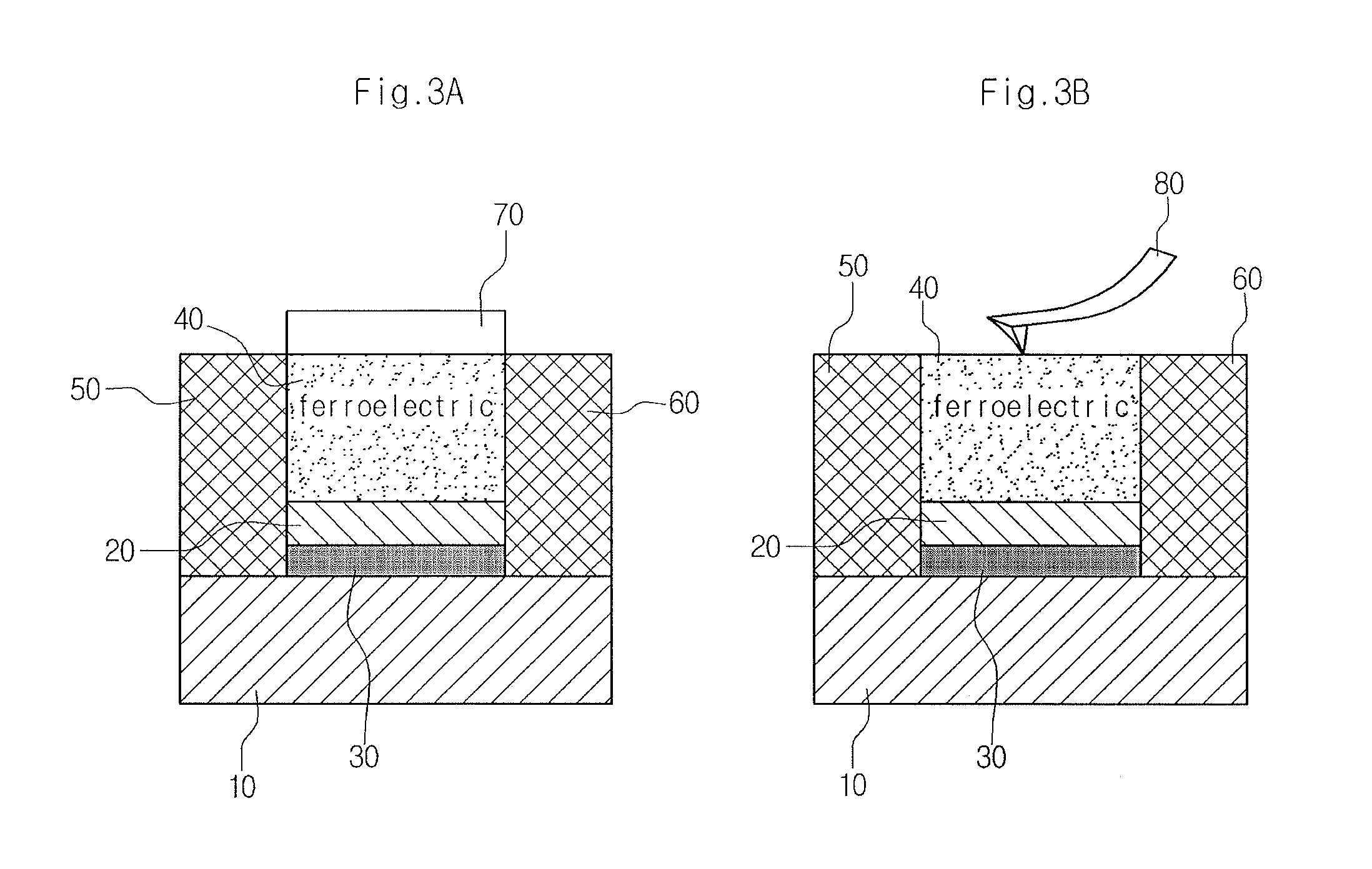
[0027]10: oxide substrate[0028]20: oxide thin film[0029]30: 2DEG conductive layer[0030]40: ferroelectric layer[0031]50: source electrode[0032]60: drain electrode[0033]70: connection electrode (metal gate electrode)[0034]80: connection electrode (conductive probe tip)

DETAILED DESCRIPTION

[0035]Exemplary embodiments now will be described more fully hereinafter with reference to the accompanying drawings, in which exemplary embodiments are shown.

[0036]FIGS. 1a and 1b are schematic sectional views of the oxide electronic device according to an embodiment, illustrating the principle of controlling electric conductivity of two-dimensional electron gas (2DEG). FIG. 2 is a molecular schematic view showing spontaneous polarization switching that occurs in a ferroelectric material. In addition, FIGS. 3a and 3b are schematic sectional views of the oxide electronic device, particularly a transistor, according to an embodiment.

[0037]Referring to FIGS. 1a and 1b, the oxide electronic device accord...


PUM

PropertyMeasurementUnit
electric conductivityaaaaaaaaaa
ferroelectricaaaaaaaaaa
structureaaaaaaaaaa

Abstract

Provided is an oxide electronic device, including: an oxide substrate; an oxide thin film layer formed on the oxide substrate and containing an oxide that is heterogeneous with respect to the oxide substrate; and a ferroelectric layer formed on the oxide thin film layer and controlling electric conductivity of two-dimensional electron gas (2DEG) generated at an interface between the oxide substrate and the oxide thin film layer. Provided also is a method for manufacturing an oxide electronic device, including: depositing, on an oxide substrate, an oxide that is heterogeneous with respect to the oxide substrate to form an oxide thin film layer; and forming a ferroelectric layer on the oxide thin film layer, wherein the ferroelectric layer controls electric conductivity of 2DEG generated at an interface between the oxide substrate and the oxide thin film layer.

Description

CROSS-REFERENCE TO RELATED APPLICATION[0001]This application claims priority to Korean Patent Application No. 10-2012-0090297, filed on Aug. 17, 2012, and all the benefits accruing therefrom under 35 U.S.C. §119, the contents of which in its entirety are herein incorporated by reference.BACKGROUND[0002]1. Field[0003]The present disclosure relates to an oxide electronic device and a method for manufacturing the same. More particularly, the present disclosure relates to an oxide electronic device, which allows electric conductivity of two-dimensional electron gas (2DEG) generated at an interface of heterogeneous oxides to be controlled stably in a non-volatile mode, as well as to a method for manufacturing the same.[0004]2. Description of the Related Art[0005]Electronic devices, such as transistors, which repeat logging and deletion of data, have high convenience. Due to this, electronic devices, such as transistors, are used widely in portable memory media, including a USB memory and...

Claims


Application Information

Patent Timeline
Patent Type & Authority Patents(United States)
IPC IPC(8): H01L29/12H01L29/66H01L29/778
CPCH01L29/778H01L29/408H01L29/516H01L29/66969H01L29/7786H01L29/24
Inventor BAEK, SEUNG HYUBKIM, SHIN IKKIM, JIN SANGCHOI, JI WONYOON, SEOK JINKANG, CHONG YUN
Owner KOREA INST OF SCI & TECH
Why Eureka
Try Eureka