Semiconductor structure and method for manufacturing the same

a technology of semiconductor devices and semiconductor components, applied in the direction of semiconductor devices, electrical devices, transistors, etc., can solve the problems of unfavorable performance and large contact resistance, and achieve the effect of enhancing the performance of the semiconductor device, reducing the capacitance, and extending the distance and reducing the area

Active Publication Date: 2014-12-09
INST OF MICROELECTRONICS CHINESE ACAD OF SCI
View PDF12 Cites 0 Cited by
  • Summary
  • Abstract
  • Description
  • Claims
  • Application Information

AI Technical Summary

Benefits of technology

[0006]The present invention aims to provide a semiconductor structure and a method for manufacturing the same, so as to reduce capacitance between a metal layer and a body silicon layer of an SOI layer.
[0014]The present invention provides a semiconductor structure and a method for manufacturing the same, which lies in forming firstly trenches extending to a BOX layer on an SOI substrate, then forming sidewall spacers on sidewalls of the trenches, and forming a metal layer inside the trenches finally; because the sidewall spacers exhibit a thickness to certain extent, thus the distance between the metal layer and the body silicon layer of the SOI substrate becomes farther; besides, the area of the metal layer facing straight to the lower surface of the body silicon layer is becomes smaller, thus the extension of distance and decrease in the area reduce the capacitance between the metal layer and the body silicon layer of the SOI substrate when the semiconductor device is in operation, which therefore favorably enhances performance of the semiconductor device.

Problems solved by technology

In the prior art, when contacts to the source / drain regions are formed on a semiconductor device using aforesaid SOI substrate, contact resistances are relatively large, since the contact area between bottoms of the contacts and the source / drain regions becomes limited with downscaling of the device size.
However, said semiconductor structure still has shortcomings, for example, when a semiconductor device manufactured from said semiconductor structure is in operation, a relatively large capacitance shall arise between the metal layer 15 and the body silicon layer 13, which unfavorably impairs the performance of the semiconductor device.

Method used


Image

  • Semiconductor structure and method for manufacturing the same
  • Semiconductor structure and method for manufacturing the same
  • Semiconductor structure and method for manufacturing the same

Examples


Embodiment Construction

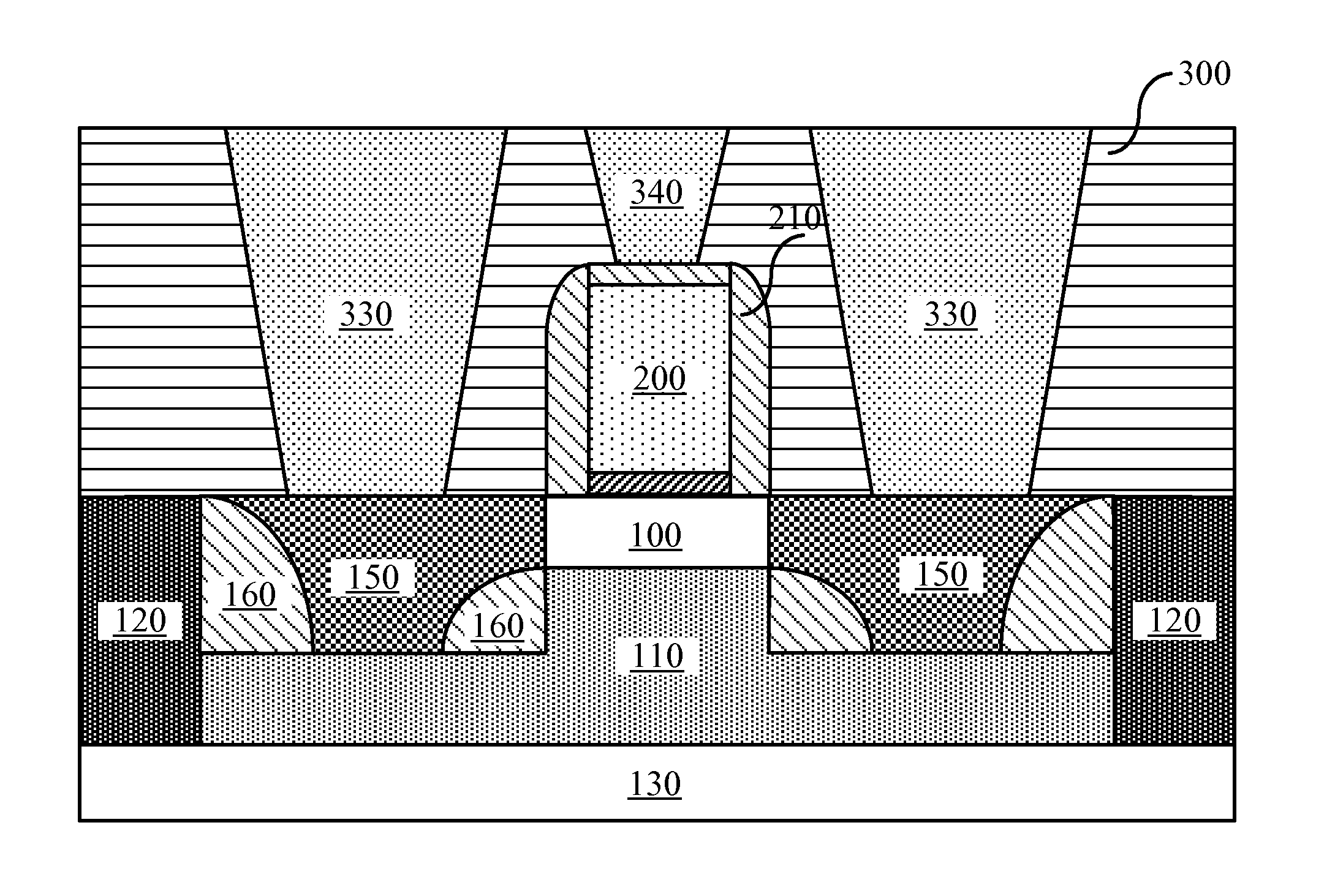
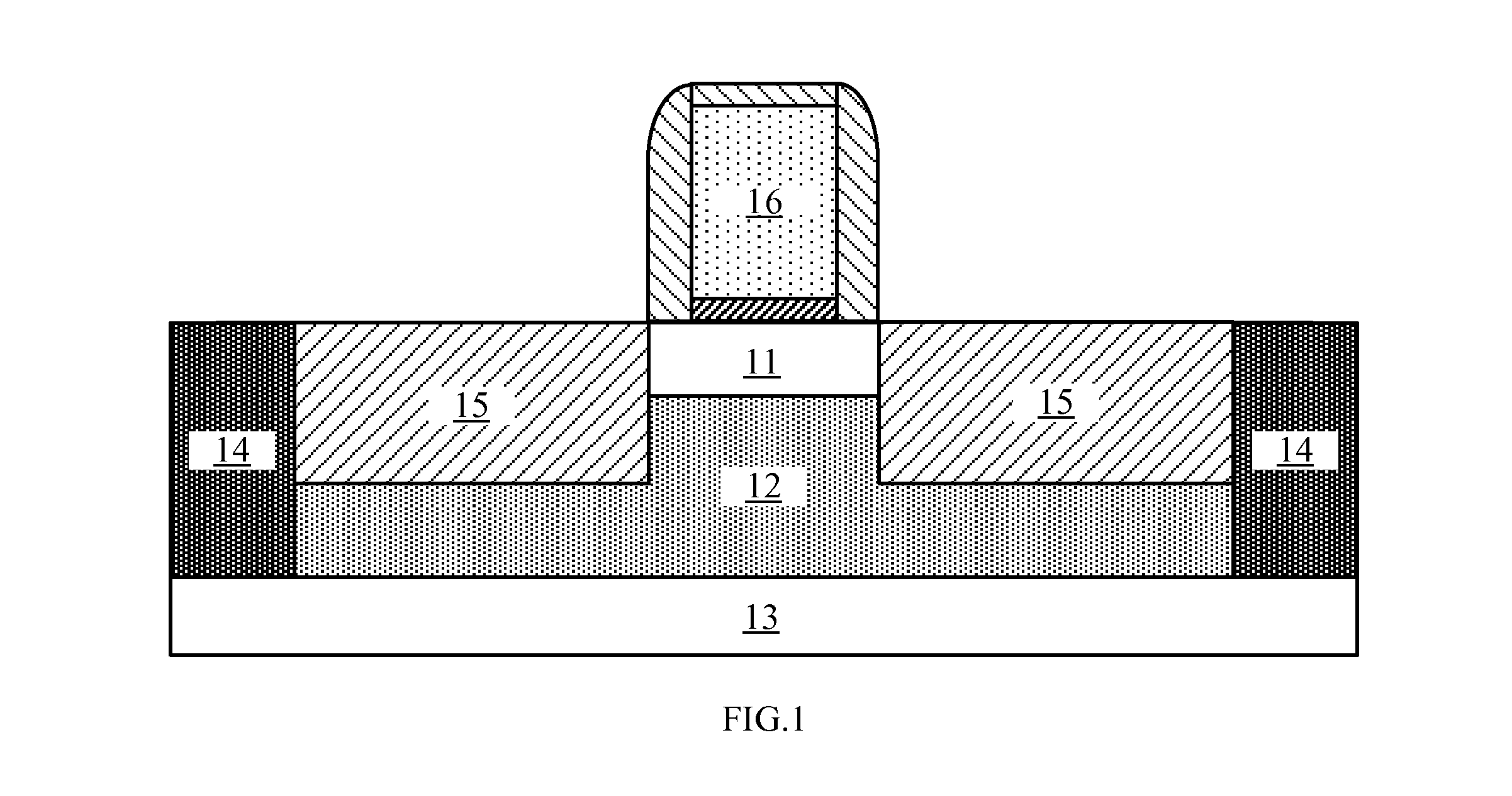
[0022]Objectives, technical solutions and advantages of the present invention are made more evident according to the following detailed description of exemplary embodiments in conjunction with the accompanying drawings.

[0023]Embodiments of the present invention are described here below, wherein examples of the embodiments are illustrated in the drawings, in which same or similar reference signs throughout denote same or similar elements or elements have same or similar functions. It should be appreciated that the embodiments described below in conjunction with the drawings are illustrative, and are provided for explaining the prevent invention only, thus shall not be interpreted as limitations to the present invention.

[0024]Various embodiments or examples are provided here below to implement different structures of the present invention. To simplify the disclosure of the present invention, description of the components and arrangements of specific examples is given below. Of course,...


PUM


Abstract

The present invention provides a method for manufacturing a semiconductor structure, which comprises: providing an SOI substrate, forming a gate structure on the SOI substrate; etching an SOI layer of the SOI substrate and a BOX layer of the SOI substrate on both sides of the gate structure to form trenches, the trenches exposing the BOX layer and extending partly into the BOX layer; forming sidewall spacers on sidewalls of the trenches; forming inside the trenches a metal layer covering the sidewall spacers, wherein the metal layer is in contact with the SOI layer which is under the gate structure. Accordingly, the present invention further provides a semiconductor structure formed according to aforesaid method. The manufacturing method and the semiconductor structure according to the present invention make it possible to reduce capacitance between a metal layer and a body silicon layer of an SOI substrate when a semiconductor device is in operation, which is therefore favorable for enhancing performance of the semiconductor device.

Description

CROSS REFERENCE TO RELATED APPLICATION[0001]This application is a National Phase application of, and claims priority to, PCT Application No. PCT / CN2011 / 078877, filed on Aug. 25, 2011, entitled “SEMICONDUCTOR STRUCTURE AND METHOD FOR MANUFACTURING THE SAME”, which claimed priority to Chinese Application No. 201110175568.3, filed on Jun. 27, 2011. Both the PCT Application and Chinese Application are incorporated herein by reference in their entireties.FIELD OF THE INVENTION[0002]The present invention relates to semiconductor manufacturing field, particularity, to a semiconductor structure and a method for manufacturing the same.BACKGROUND OF THE INVENTION[0003]With development in the semiconductor manufacturing industry, integrated circuits with better performance and more powerful functions require greater element density; besides, sizes of and spaces between the components have to be further scaled down (which has already reached the nanometer-level nowadays). Accordingly, various m...

Claims


Application Information

Patent Timeline
Patent Type & Authority Patents(United States)
IPC IPC(8): H01L29/423H01L21/28H01L29/417H01L29/78H01L29/66
CPCH01L29/66772H01L29/41733H01L29/4232H01L29/7839H01L29/78H01L21/28008H01L29/66643H01L29/66545
Inventor YIN, HAIZHOUZHU, HUILONGLUO, ZHIJIONG
Owner INST OF MICROELECTRONICS CHINESE ACAD OF SCI
Why Eureka
Try Eureka