
Overcoming chip warping to enhance wetting of solder bumps and flip chip attaches in a flip chip package

a flip chip and flip chip technology, applied in the incorporation of printed electric components, electrical apparatus construction details, basic electric elements, etc., can solve the problems of warping of ic chips and chip carriers, poor quality of electrical contacts between previously solidified solder contacts, and greater complexity of semiconductor packaging design

Inactive Publication Date: 2015-01-06
GLOBALFOUNDRIES U S INC
View PDF15 Cites 4 Cited by
  • Summary
  • Abstract
  • Description
  • Claims
  • Application Information

AI Technical Summary

Benefits of technology

The solution significantly reduces warpage, enhancing the probability of wetting between solder bumps and FC attaches, thereby improving the quality and reliability of electrical connections in flip chip packages.

Problems solved by technology

The combination of these requirements results in greater complexity of semiconductor packaging design.
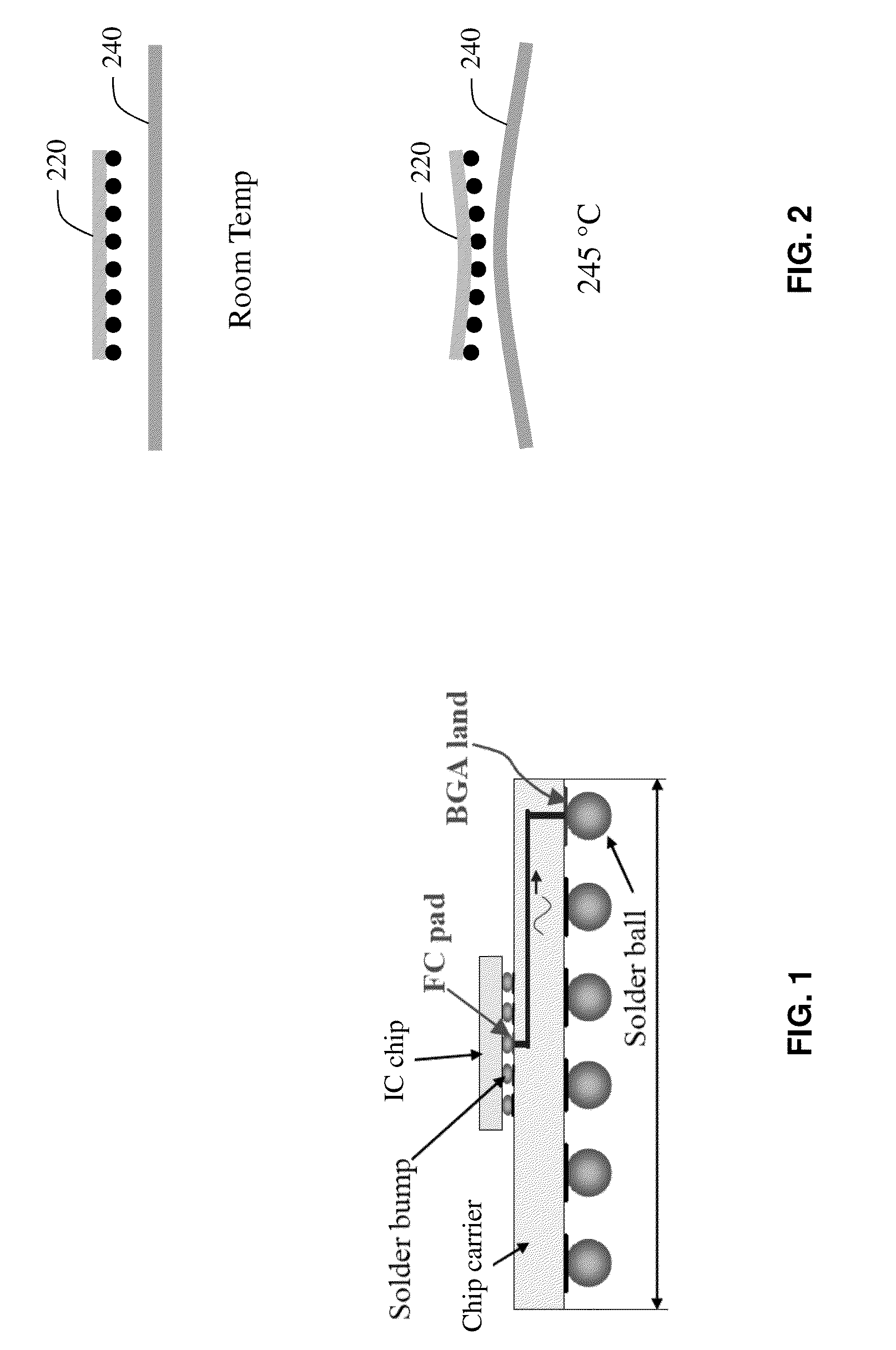
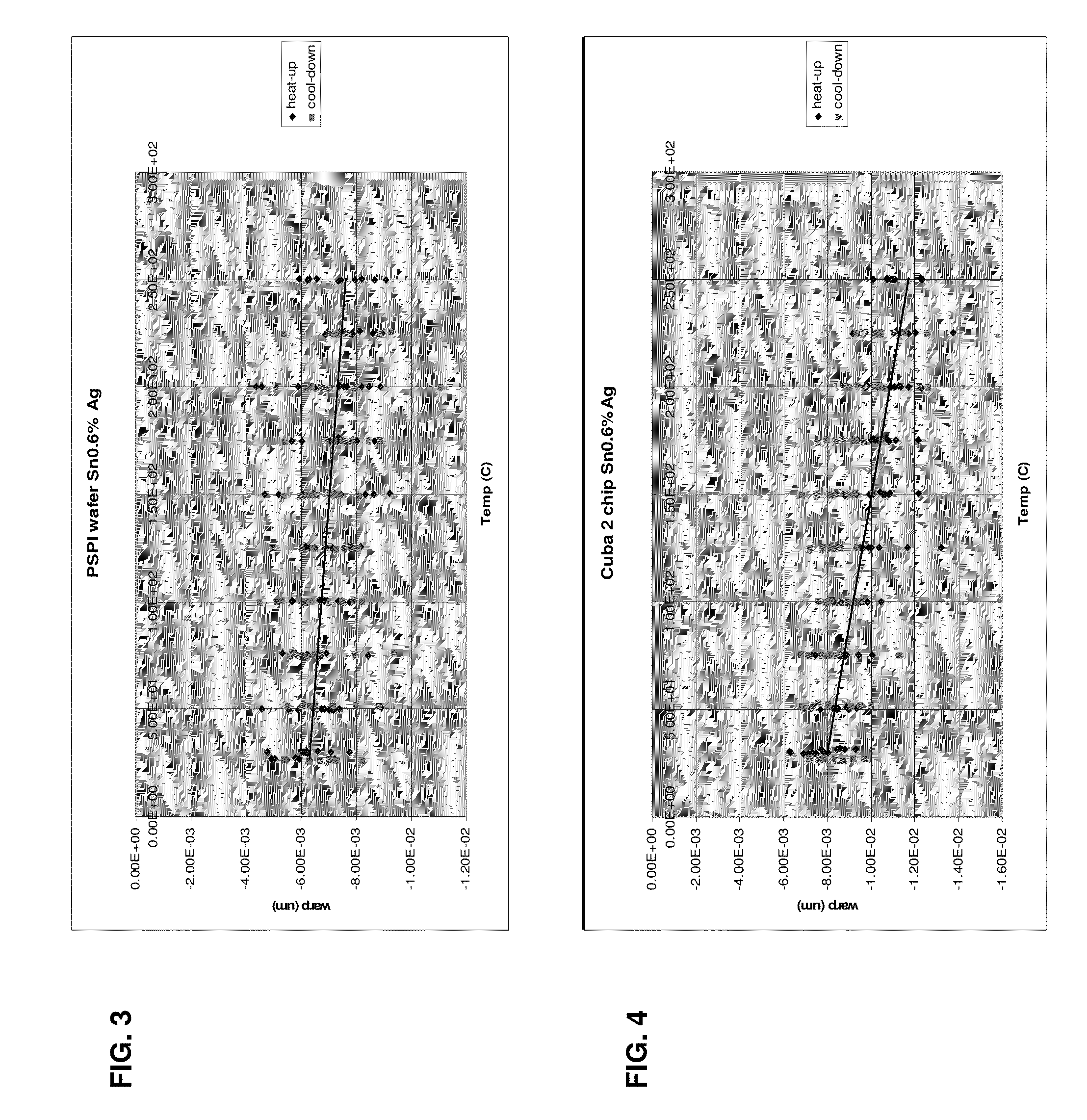
During heating, both the IC chip and the chip carrier can warp because of mismatches between the coefficients of thermal expansion (CTE) of their constituent layers.
However, the quality of the electrical contacts between these previously solidified solder contacts is not as good as that of “wetted” contacts between the two opposing miscible solders of the heated solder bumps of the IC chip and the heated solder layers of the FC attaches.

Method used


Image

  • Overcoming chip warping to enhance wetting of solder bumps and flip chip attaches in a flip chip package
  • Overcoming chip warping to enhance wetting of solder bumps and flip chip attaches in a flip chip package
  • Overcoming chip warping to enhance wetting of solder bumps and flip chip attaches in a flip chip package

Examples


Embodiment Construction

[0027]The exemplary embodiments of the disclosure and their various features and advantageous details are explained more fully with reference to the non-limiting exemplary embodiments that are illustrated in the accompanying drawings and detailed in the following description. It should be noted that the features illustrated in the drawings are not necessarily drawn to scale. Descriptions of well-known materials, components, and processing techniques are omitted so as to not unnecessarily obscure the exemplary embodiments of the disclosure. The examples used herein are intended to merely facilitate an understanding of ways in which the exemplary embodiments of the disclosure may be practiced and to further enable those of skill in the art to practice the exemplary embodiments of the disclosure. Accordingly, the examples should not be construed as limiting the scope of the exemplary embodiments of the disclosure.

[0028]As described above, there remains a need to reliably form a “wet” c...


PUM


Abstract

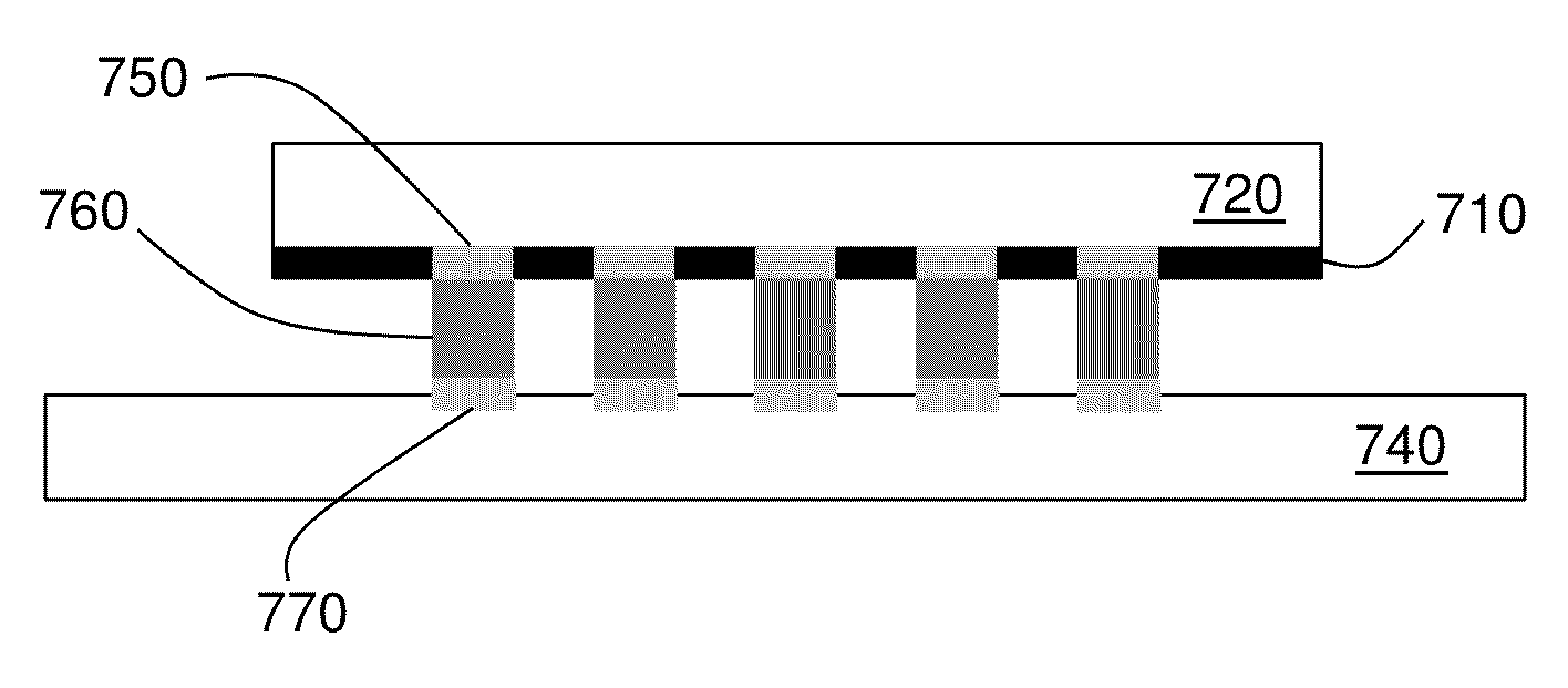
Structures and methods for forming good electrical connections between an integrated circuit (IC) chip and a chip carrier of a flip chip package include forming one of: a tensile layer on a front side of the IC chip, which faces a tops surface of the chip carrier, and a compressive layer on the backside of the IC chip. Addition of one of: a tensile layer to the front side of the IC chip and a compressive layer the backside of the IC chip, may reduce or modulate warpage of the IC chip and enhance wetting of opposing solder surfaces of solder bumps on the IC chip and solder formed on flip chip (FC) attaches of a chip carrier during making of the flip chip package.

Description

BACKGROUND[0001]1. Field of the Invention[0002]This disclosure generally relates to structures and methods for forming good electrical connections between an integrated circuit (IC) chip and a chip carrier of a flip chip package. More particularly, addition of one of: tensile layers and a compressive layer, to selected surfaces of IC chips in a wafer prior to solder bump re-heating, may reduce or modulate warpage of the IC chip and enhance wetting of opposing solder surfaces of solder bumps on the IC chip and solder formed on flip chip (FC) attaches of a chip carrier in a flip chip package.[0003]2. Description of Related Art[0004]The semiconductor marketplace continues to demand smaller devices, which require greater connectivity densities for packaging design. The increased functionality of smaller semiconductor devices requires an increased number of signal, power, and ground connections, and a corresponding decrease in connection pitch is required to maintain reasonable chip size...

Claims


Application Information

Patent Timeline
Patent Type & Authority Patents(United States)
IPC IPC(8): H01L23/48H01L21/60
CPCH01L2924/15174H01L2924/15311H01L2224/11011H01L23/291H01L23/293H01L23/3164H01L24/11H01L24/13H01L24/16H01L24/81H01L2224/11001H01L2224/1131H01L2224/11849H01L2224/16227H01L2224/81007H01L2224/81191H01L2224/13111H01L2924/3511H01L2224/16225H01L2924/12042H01L2924/00014H01L2924/00012H01L2924/01047H01L2924/00
Inventor DAUBENSPECK, TIMOTHY H.GAMBINO, JEFFREY P.MUZZY, CHRISTOPHER D.NORMAND, NATHALIEQUESTAD, DAVID L.SAUTER, WOLFGANGSULLIVAN, TIMOTHY D.
Owner GLOBALFOUNDRIES U S INC
Learn More