CMOS image sensor with global shutter, rolling shutter, and a variable conversion gain, having pixels employing several BCMD transistors coupled to a single photodiode and dual gate BCMD transistors for charge storage and sensing

a global shutter and image sensor technology, applied in transistors, television system scanning details, television systems, etc., can solve problems such as undesirable picture distortion, exposure time skew, and sequential scanning of pixels after charge accumulates in them

Active Publication Date: 2015-01-06
SEMICON COMPONENTS IND LLC
View PDF11 Cites 19 Cited by
  • Summary
  • Abstract
  • Description
  • Claims
  • Application Information

AI Technical Summary

Problems solved by technology

The principal disadvantage of the standard CMOS sensors is that pixel scanning after charge has been accumulated in them is performed in a sequential manner row by row.
This generates exposure time skew, which can be observed in the pictures of moving objects and which causes an undesirable picture distortion.
High dark current in the storage sites would also add to noise and also would generate undesirable shading effects in the picture that would have to be compensated for.
Unfortunately, the second pinned photodiode consumes a significant valuable pixel area, thus increasing the size of the sensor and ultimately its cost.

Method used


Image

  • CMOS image sensor with global shutter, rolling shutter, and a variable conversion gain, having pixels employing several BCMD transistors coupled to a single photodiode and dual gate BCMD transistors for charge storage and sensing
  • CMOS image sensor with global shutter, rolling shutter, and a variable conversion gain, having pixels employing several BCMD transistors coupled to a single photodiode and dual gate BCMD transistors for charge storage and sensing
  • CMOS image sensor with global shutter, rolling shutter, and a variable conversion gain, having pixels employing several BCMD transistors coupled to a single photodiode and dual gate BCMD transistors for charge storage and sensing

Examples


Embodiment Construction

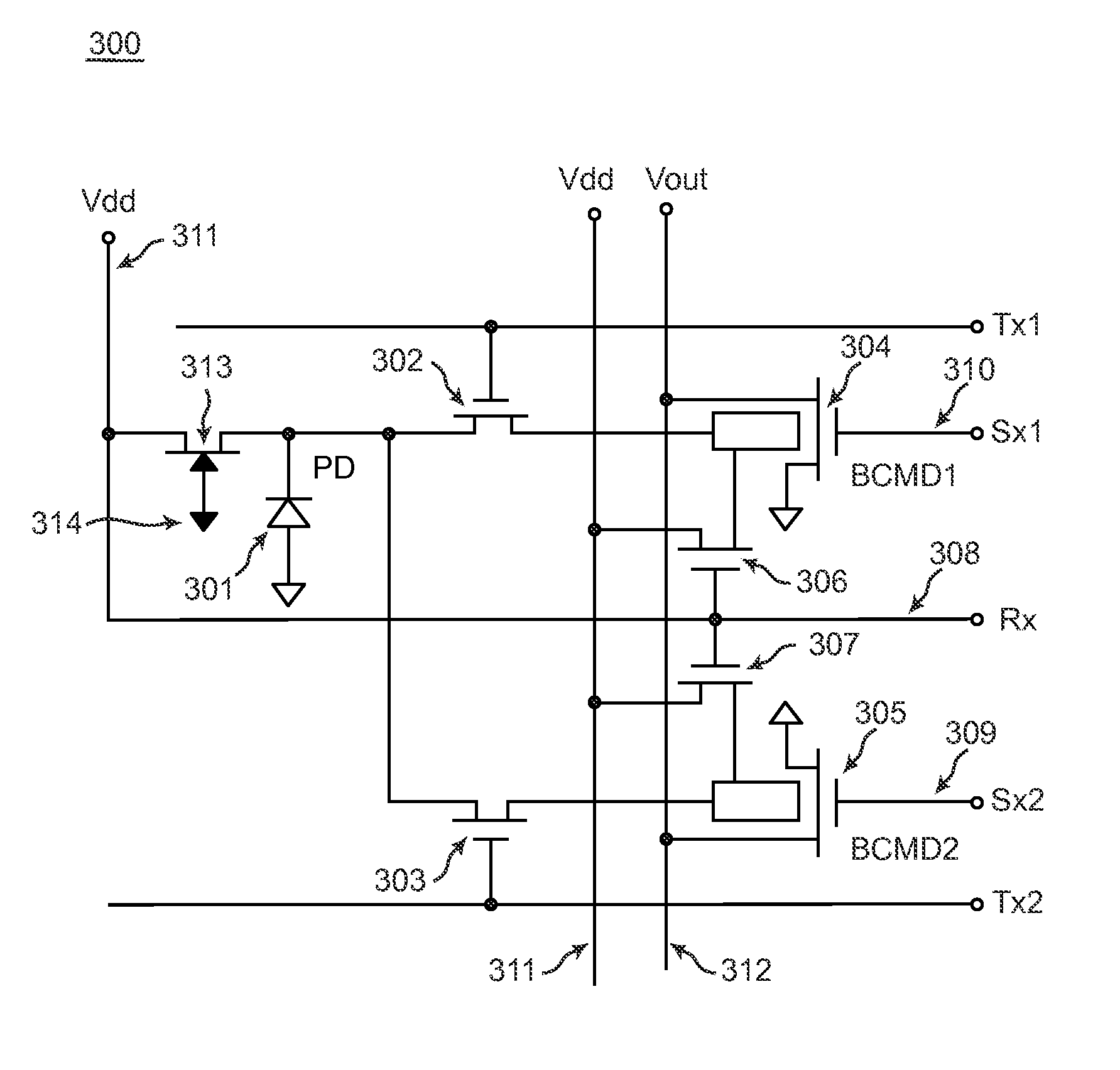
[0021]The drawing of FIG. 3 represents a simplified circuit diagram 300 of a CMOS sensor pixel that consists of a pinned photodiode 301 interfaced with two transfer gates 302 and 303 that transfer charge into two different BCMD transistors 304 and 305 respectively. The BCMD transistors 304 and 305 are reset by the reset transistors 306 and 307 when a reset pulse is applied to row reset gate bus 308. The BCMD transistors 304 and 305 are addressed by applying suitable biases to their gates through row address lines 309 and 310. A reset drain voltage is applied to this pixel through column bias line 311 and the output appears on column output line 312. From this simplified circuit schematic it is clear how the pixel operates. For low level signals, when during the long integration time enough charge accumulates in the pixel, it is no problem to transfer it into one BCMD transistor for storage and readout. However, when a high level signal is accumulated during the long integration time...


PUM


Abstract

The invention describes a solid-state CMOS image sensor array and discloses image sensor array pixels with global and rolling shutter capabilities that utilize multiple BCMD transistors for a single photodiode, for charge storage and sensing. Thus, the valuable pixel area saved by employing the BCMD transistor for charge storage and sensing is used by placing several BCMD transistors coupled to one photodiode. This increases the Dynamic Range (DR) of the sensor, since the same photodiode can integrate charge for different integration times, both long and short. This allows sensing of two different image signals from a single pixel without saturation, a low level signal with long integration time followed by a high level signal with short integration time. The signal processing circuits located at the periphery of the array can then process these signals into a single Wide Dynamic Range (WDR) output. Further disclosed is an image sensor array with pixels that use BCMD transistors for charge storage and sensing having multiple concentric gates, which allows changing the conversion gain of the BCMD transistors by applying various biases to the gates. Variable conversion gain is a useful feature when building WDR sensors since low conversion gain and high well capacity allows detection of high level signals and the same structure can be used to detect, at the same time, low level signals with high conversion gain and thus low noise.

Description

CROSS REFERENCE TO RELATED APPLICATION[0001]This application claims priority under 35 USC Sec. 119(e)(1) of provisional application No. 61 / 438,036 filed on Jan. 31, 2011.BACKGROUND OF THE INVENTION[0002]1. Field of the Invention[0003]The disclosed invention relates to solid-state image sensors and more particularly to small pixel size CMOS image sensors with both global and rolling shutter capability that incorporate BCMD transistors in the pixels with lateral or vertical reset for charge storage and sensing.[0004]2. Description of Related Art[0005]Typical image sensors sense light by converting impinging photons into electrons that are integrated (collected) in sensor pixels. After completion of an integration cycle collected charge is converted into a voltage, which is supplied to the output terminals of the sensor. In CMOS image sensors the charge to voltage conversion is accomplished directly in the pixels themselves and the analog pixel voltage is transferred to the output term...

Claims


Application Information

Patent Timeline
Patent Type & Authority Patents(United States)
IPC IPC(8): H04N5/335H04N5/359H04N5/3745
CPCH04N5/3591H04N5/3745H01L27/14614H01L27/14605H01L27/14679H01L27/14656H04N25/621H04N25/77H01L27/14612H01L27/14645
Inventor HYNECEK, JAROSLAVAGRANOV, GENNADIYLI, XIANGLIKOMORI, HIROFUMIZHAO, XIAWAN, CHUNG CHUN
Owner SEMICON COMPONENTS IND LLC
Why Eureka
Try Eureka