Chopped Hall effect sensor

a sensor and hall effect technology, applied in special purpose recording/indication devices, magnetic measurements, instruments, etc., can solve the problems of reducing the ripple effect, slowing down the sensor response time, and imbalanced hall effect elements or plates

Active Publication Date: 2008-09-16
ALLEGRO MICROSYSTEMS INC
View PDF5 Cites 135 Cited by
  • Summary
  • Abstract
  • Description
  • Claims
  • Application Information

AI Technical Summary

Benefits of technology

[0010]With this arrangement, the Hall effect sensor is provided with fast response time through the use of the selective filter that removes the offset signal component with its associated ripple, thereby eliminating the significant low pass filtering requirements of some conventional chopped Hall effect sensors. A high signal to noise ratio is achieved with the use of the anti-aliasing filter that removes frequency components above a predetermined frequency, so that the selective filter meets the Nyquist criterion for noise signals, thereby reducing baseband noise by preventing aliasing.
[0011]In embodiments in which the offset signal component is modulated by the modulation circuit, an even number of additional modulation circuits are provided between the output of the Hall plate modulation circuit and the input to the filter. In this way, the offset signal component is modulated when it reaches the selective filter for removal. Alternatively, in embodiments in which the magnetic signal component is modulated, the amplifier includes an odd number of additional modulation circuits between the output of the Hall plate modulation circuit and the input to the filter, again ensuring that the offset signal component is modulated when it reaches the selective filter for removal.

Problems solved by technology

Hall effect elements or plates experience imbalances due to resistance gradients, geometrical asymmetries and piezoresistive effects which can introduce an offset voltage.
While this technique is effective to remove the Hall offset voltage, the resulting ripple on the sensor output signal and the sensor response time must be balanced since, the more filtering applied, the lower the resulting ripple, but also the slower the sensor response time.
This is because the sampling and holding operation can produce noise fold back (i.e., aliasing) since the baseband noise is undersampled.

Method used


Image

  • Chopped Hall effect sensor
  • Chopped Hall effect sensor
  • Chopped Hall effect sensor

Examples


Embodiment Construction

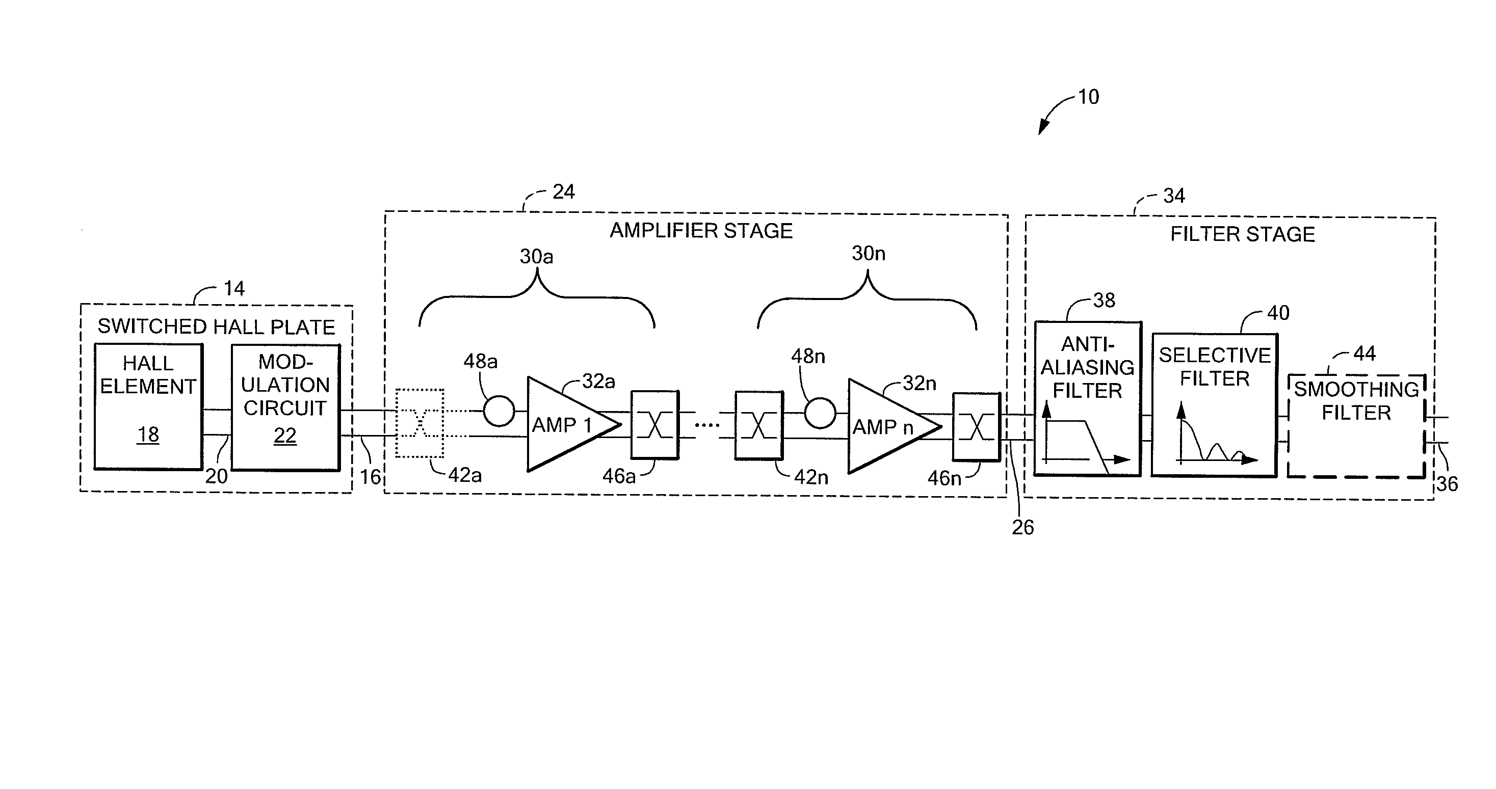
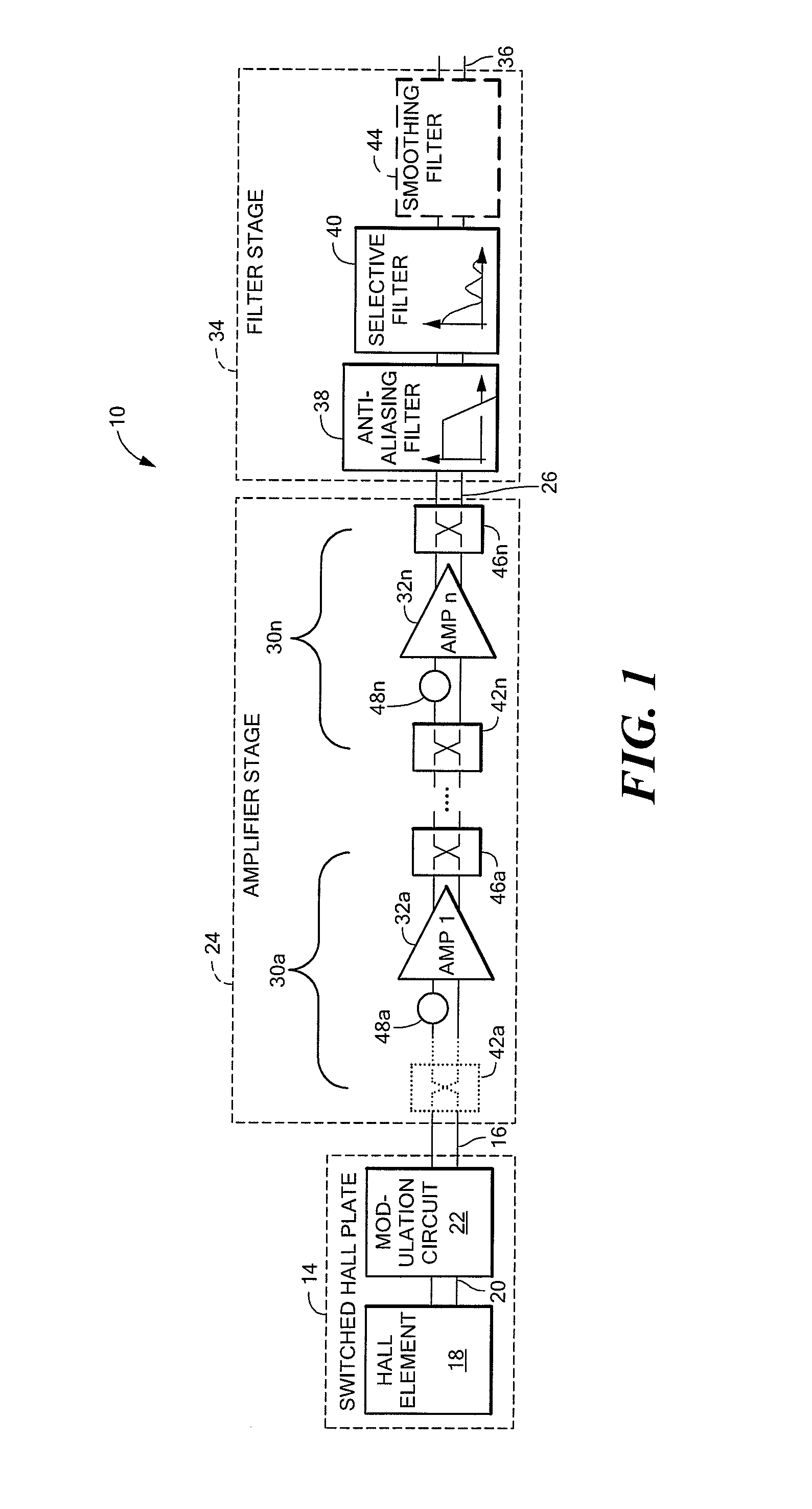
[0045]Referring to FIG. 1, a chopped Hall effect sensor 10 includes a switched Hall plate 14 providing a switched Hall output signal 16, an amplifier stage 24 having an input responsive to the switched Hall output signal 16 and an output at which is provided an amplifier output signal 26, and a filter stage 34 having an input responsive to the amplifier output signal 26 and an output at which is provided a sensor output signal 36. The filter stage 34 includes an anti-aliasing filter 38 and a selective filter 40, as shown.

[0046]With this arrangement, the Hall effect sensor 10 is provided with low noise and fast response time. Fast response time is achieved with the use of the selective filter 40 that removes the offset signal component with its associated ripple, thereby eliminating the significant low pass filtering requirements of some conventional chopped Hall effect sensors. A high signal to noise ratio is achieved with the use of the anti-aliasing filter 38 to remove frequency c...


PUM


Abstract

A chopped Hall effect sensor topology includes a switched Hall plate, an amplifier responsive to an output of the switched Hall plate and a filter stage responsive to the output of the amplifier and including an anti-aliasing filter and a selective filter that is tuned to the modulation frequency. The switched Hall plate includes a Hall element and a Hall plate modulation circuit that modulates the Hall offset signal component or the magnetic signal component. In embodiments in which the Hall offset signal component is modulated by the switched Hall plate, the amplifier, if chopped, includes an even number of additional modulation circuits. In embodiments in which the magnetic signal component is modulated by the switched Hall plate, the amplifier contains an odd number of modulation circuits. The described topology provides a low noise, fast response time Hall effect sensor.

Description

CROSS REFERENCE TO RELATED APPLICATIONS[0001]Not Applicable.STATEMENT REGARDING FEDERALLY SPONSORED RESEARCH[0002]Not Applicable.FIELD OF THE INVENTION[0003]This invention relates generally to Hall effect sensors and, more particularly, to a chopped Hall effect sensor having fast response time and reduced noise.BACKGROUND OF THE INVENTION[0004]Hall effect sensors are used in a wide variety of applications including industrial and consumer applications. As one example, Hall effect sensors are widely used in the automotive industry for mechanical position sensing, such as gear tooth sensors used in brake systems. Such applications require accuracy.[0005]Hall effect elements or plates experience imbalances due to resistance gradients, geometrical asymmetries and piezoresistive effects which can introduce an offset voltage. The magnitude and polarity of the offset voltage are a function of stresses in the semiconductor from which the element is formed, which stresses vary with mechanica...

Claims


Application Information

Patent Timeline
Patent Type & Authority Patents(United States)
IPC IPC(8): G01R33/07
CPCG01D3/02G01R33/07G01R33/02G06M1/274
Inventor MONREAL, GERARDOROMERO, HERNAN D.
Owner ALLEGRO MICROSYSTEMS INC
Why Eureka
Try Eureka