Flash memory device

a flash memory and memory technology, applied in the field of semiconductor memory devices, can solve problems such as wrong programming of conventional flash memory devices, and achieve the effect of improving programming accuracy and accurate programming

Active Publication Date: 2015-01-27
SHANGHAI HUAHONG GRACE SEMICON MFG CORP
View PDF6 Cites 1 Cited by
  • Summary
  • Abstract
  • Description
  • Claims
  • Application Information

AI Technical Summary

Benefits of technology

[0013]Due to the voltage stabilizing unit, in a programming process, the voltage applied to the bit lines which are not related with programming may not drop as a result of current leakage. Therefore, the memory cells except the memory cell to be programmed are kept in cut off state, without a current passing. As a result, interference with the memory cells which are not to be programmed may be effectively avoided and the accuracy of programming may be improved.
[0014]Furthermore, in an alternative embodiment, the bias unit can precisely control the voltage applied to the bit lines, which lead to a more accurate programming.

Problems solved by technology

However, conventional flash memory devices suffer from wrongly programming due to leakage current on bit lines.

Method used


Image

  • Flash memory device
  • Flash memory device
  • Flash memory device

Examples


Embodiment Construction

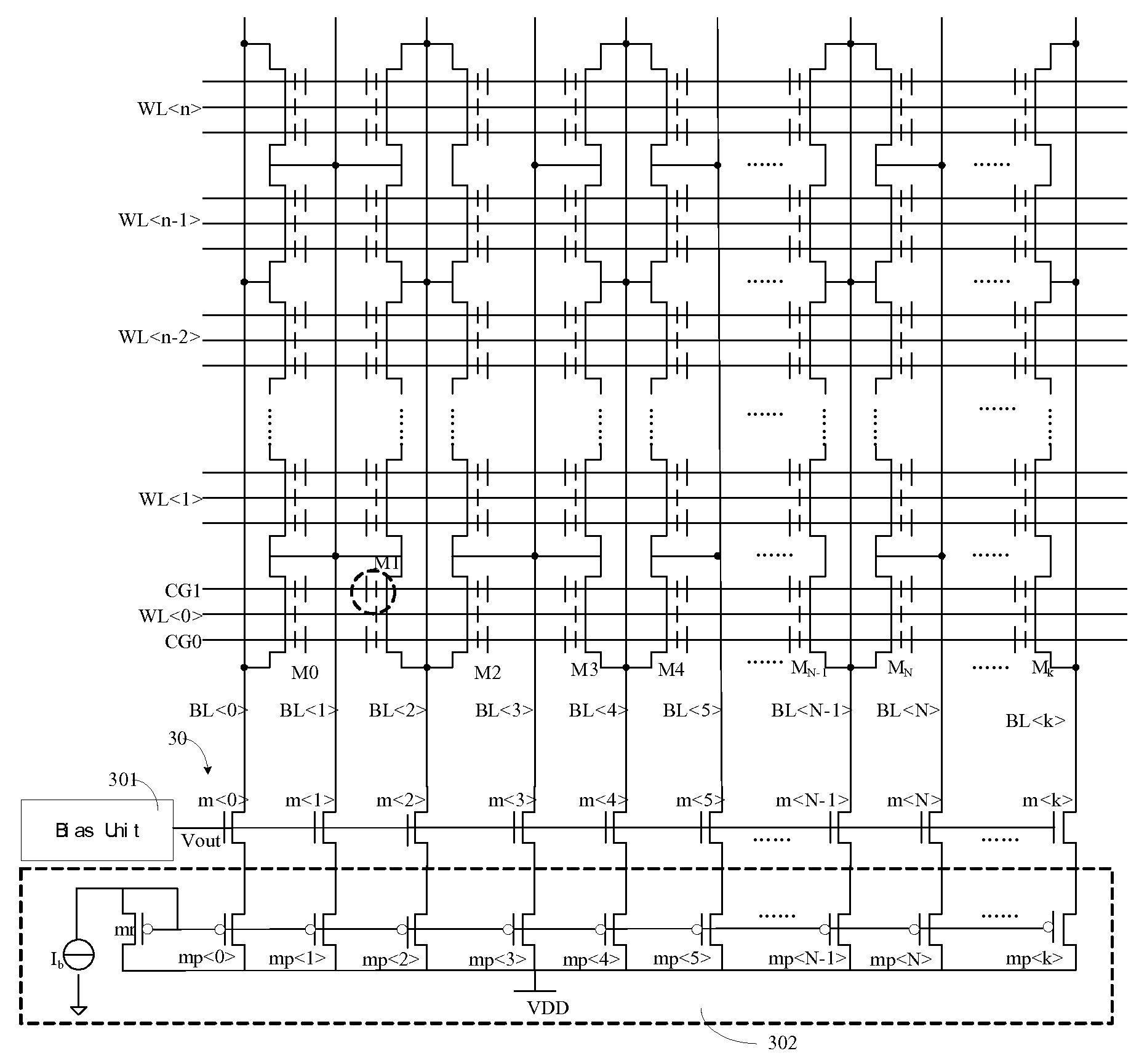
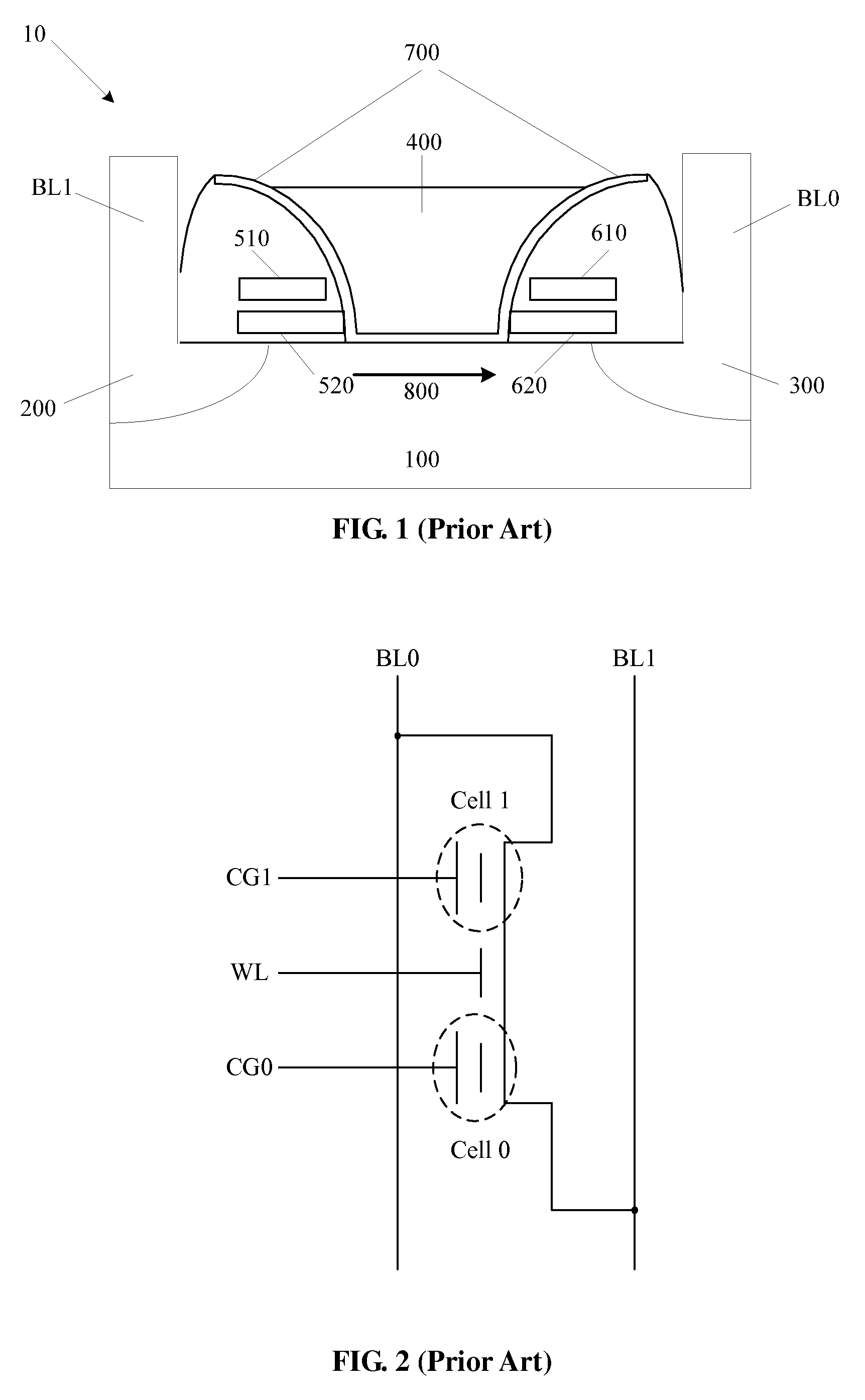
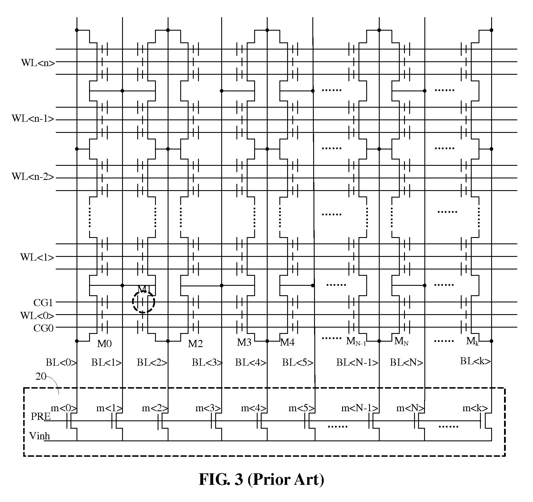
[0020]FIG. 1 is a schematic cross-sectional view of a conventional split-gate memory cell. FIG. 2 is an equivalent circuit structure of the split-gate memory cell as shown in FIG. 1. Referring to FIGS. 1 and 2, a memory cell 10 includes: a substrate 100; a source region 200 and a drain region 300 configured in the substrate; a channel region 800 between the source region 200 and the drain region 300; a first floating gate 520 and a first control gate 510 (shown as “CG0” in FIG. 2) on the substrate, a second floating gate 620 and a second control gate 610 (shown as “CG1” in FIG. 2) on the substrate; an oxide layer 700 insulating the first floating gate 520 and the second floating gate 620; and a selection gate 400 on the oxide layer 700. The source region 200 and the drain region 300 are respectively coupled to bit lines BL1 and BL0.

[0021]Referring still to FIGS. 1 and 2, the memory cell 10 includes two sub-memory cells “cell 0” and “cell 1” respectively corresponding to the two floa...


PUM


Abstract

A flash memory device is provided. The flash memory device includes a memory cell array and a pre-charge unit. The pre-charge unit, coupled to a plurality of bit lines corresponding with the memory cell array, pre-charges the bit lines to a predetermined voltage during a pre-charge stage. The pre-charge unit includes a voltage stabilizing unit to provide a constant current to the bit lines. Due to the voltage stabilizing unit, in a programming process, the voltage applied to the bit lines which are not related with programming may not drop as a result of current leakage. Therefore, the memory cells except the memory cell to be programmed are kept in cut off state, without a current passing. As a result, interference with the memory cells which are not to be programmed may be effectively avoided and the accuracy of programming may be improved.

Description

[0001]The present application claims priority to Chinese Patent Application No. 201110300758.3, filed on Sep. 28, 2011 and entitled “FLASH MEMORY DEVICE”, the entire disclosure of which is incorporated herein by reference in its entirety.FIELD OF THE INVENTION[0002]The present disclosure generally relates to a semiconductor memory device, and more particularly, to a flash memory device.BACKGROUND OF THE INVENTION[0003]Memory devices are utilized for storage of mass data information. Currently, a variety of memory devices have been developed, for example, random access memory (RAM), dynamic random access memory (DRAM), erasable programmable read only memory (EPROM), flash memory, and the like, among which, flash memory are mainstream of nonvolatile semiconductor memories. Currently, according to structures of memory cells, flash memory are classified into stack-gate flash memory and split-gate flash memory, wherein the split-gate memory devices are widely used because of its high pro...

Claims


Application Information

Patent Timeline
Patent Type & Authority Patents(United States)
IPC IPC(8): G11C16/24G11C16/04G11C16/34
CPCG11C16/24G11C16/0425G11C16/3418
Inventor YANG, GUANGJUN
Owner SHANGHAI HUAHONG GRACE SEMICON MFG CORP
Why Eureka
Try Eureka