Semiconductor device and memory system

a memory system and semiconductor technology, applied in semiconductor devices, digital storage, instruments, etc., can solve the problems of increasing the current in the data bus, difficult to reduce the line impedance of the power supply, and large value, so as to avoid the influence of power supply noise, reduce line impedance, and obtain a distance easily

Active Publication Date: 2015-02-24
LONGITUDE LICENSING LTD
View PDF6 Cites 4 Cited by
  • Summary
  • Abstract
  • Description
  • Claims
  • Application Information

AI Technical Summary

Benefits of technology

[0010]In the semiconductor device of the invention, since operation frequencies in the first circuit region for driving the data bus and the second circuit region for performing parallel-serial conversion are different from each other, it is possible to achieve a wiring structure capable of reliably separating the first and second power supplies in the first and second circuit regions based on a difference in arrangement of the first through electrode group for the first power supply supplied to the first circuit region and the second through electrode group for the second power supply supplied to the second circuit region, in order to avoid influence of power supply noise that becomes a problem in an operation with a common power supply. That is, since the first and second through electrode groups can differ in position and orientation from each other, it is possible to easily obtain a distance by which mutual interference is suppressed and to reduce line impedance by increasing the degree of freedom of wiring layout, when forming lines of the power supplies in wiring layers. Thereby, the influence of noise between the first and second circuit regions is suppressed, and throughput of data transfer can be improved even when the number of bits of the data bus and the operation frequency are respectively increased.

Problems solved by technology

Further, the high-speed operation of these circuits requires measures against an increase in consumption current, influence of power supply noise between the circuits, and the like.
However, this causes a problem that the consumption current in the data bus increases in proportion to the number of bits of the data bus and the operating frequency respectively, which reaches an extremely larger value.
Further, when driving many data buses in a data bus region, driving timings thereof overlap so as to increase temporal variation of the consumption current, and therefore this likely becomes power supply noise that affects the operation of the I / O circuit.
Further, it is not easy to reduce line impedance of the power supplies in the data bus region and an I / O region for the purpose of dealing with such problems, since wiring structure is restricted in the DRAM core of which integration has been advanced.

Method used


Image

  • Semiconductor device and memory system
  • Semiconductor device and memory system
  • Semiconductor device and memory system

Examples


Embodiment Construction

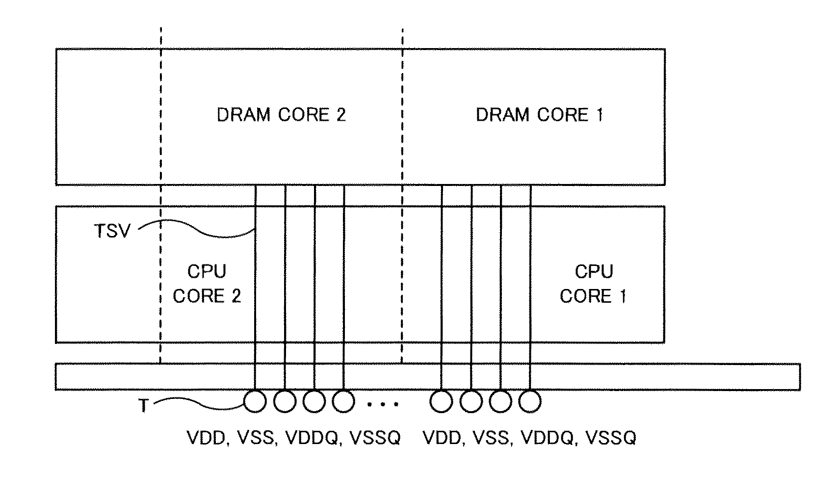
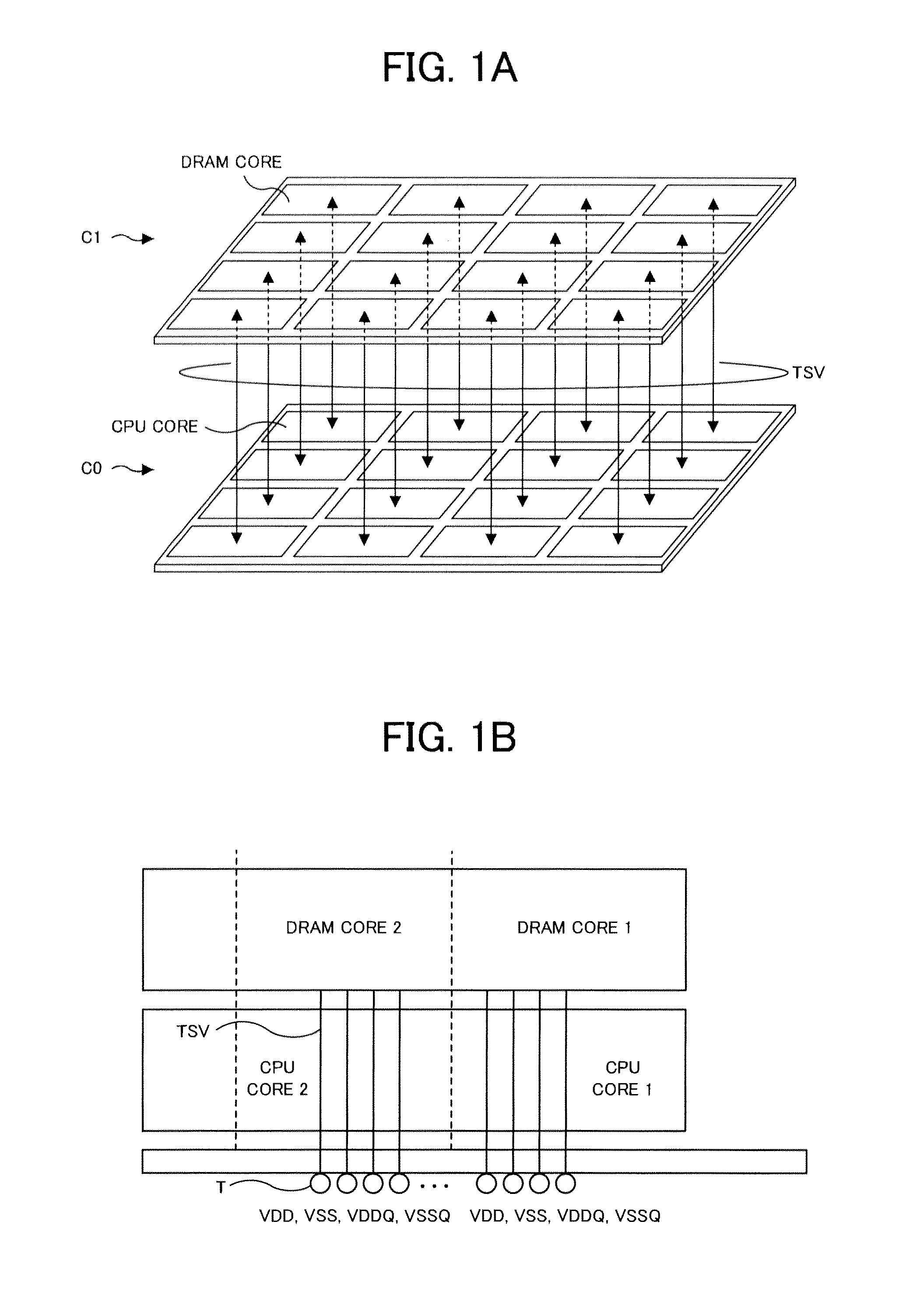
[0026]In the following, embodiments of a system will be described. In the embodiments, the invention is applied to a system comprising a multi-core DRAM chip stacked using TSVs (Through Silicon Vias) as through electrodes.

[0027]FIGS. 1A and 1B are conceptual diagrams explaining the system of an embodiment. In the system shown in FIG. 1A, a multi-core CPU chip C0 including a plurality of CPU cores and a multi-core DRAM chip C1 including a plurality of DRAM cores are stacked, and each of the CPU cores is electrically connected to a corresponding one of the DRAM cores by a plurality of TSVs. Each CPU core is a functional unit of the multi-core CPU chip C0, and each DRAM core is a functional unit of the multi-core DRAM chip C1. Each DRAM core of the multi-core DRAM chip C1 functions as a main memory, a DRAM local memory or a cache memory of a corresponding CPU core of the multi-core CPU chip C0, and data and control signals are transmitted between each CPU core and the corresponding DRA...


PUM


Abstract

A semiconductor device is disclosed in which a plurality of memory cores are provided on a semiconductor chip. Each of the memory cores comprises: first and second circuit regions and a first and second through electrode groups. a first power supply is supplied in the first circuit region in which a data bus for parallel data is driven, and a second power supply separated from the first power supply is supplied in the second circuit region in which the parallel data and serial data are bidirectionally converted. The first through electrode group includes through electrodes supplying the first power supply to the first circuit region, and the second through electrode group includes through electrodes supplying the second power supply to the second circuit region.

Description

CROSS-REFERENCE TO RELATED PATENT APPLICATIONS[0001]This application claims priority to Japanese patent application no. 2011-217658, filed Sep. 30, 2011, the entire contents of which is incorporated herein by reference.BACKGROUND OF THE INVENTION[0002]1. Field of the Invention[0003]The present invention relates to a semiconductor device comprising a plurality of memory cores implemented on a semiconductor chip, and a system in which the semiconductor chip and a control chip are stacked.[0004]2. Description of Related Art[0005]In recent years, a system has been proposed in which a multi-core memory including a plurality of memory cores is configured and a three-dimensional stacked structure is formed using through electrodes (TSVs: Through Silicon Vias) (for example, see Non-Patent Reference 1). Assuming a multi-core DRAM chip in which such a structure is applied to DRAM (Dynamic Random Access Memory), each DRAM core included in the multi-core DRAM chip is required to perform high-sp...

Claims


Application Information

Patent Timeline
Patent Type & Authority Patents(United States)
IPC IPC(8): G11C7/00G11C5/02G11C5/04G11C5/06G11C5/14G11C7/02G11C7/10G11C11/4074G11C11/4076G11C11/4096H01L23/498H01L25/065H01L25/18
CPCG11C7/1012H01L23/498G11C5/025G11C5/063G11C7/1006G11C11/4074G11C11/4076G11C11/4096H01L25/0657G11C7/02G11C5/02G11C5/04G11C5/14H01L25/18G11C2207/107H01L2225/06513H01L2225/06541H01L2924/0002H01L2924/00
Inventor KAJIGAYA, KAZUHIKOONO, KAZUOSEKIGUCHI, TOMONORI
Owner LONGITUDE LICENSING LTD
Why Eureka
Try Eureka