
Methods for reproducible flash layer deposition

a flash layer and deposition method technology, applied in the direction of capacitor details, electrical equipment, capacitors, etc., can solve the problems of achieve the effect of reducing the leakage current, improving the k-value of the high-k dielectric layer, and reducing the deposition ra

Inactive Publication Date: 2015-04-21
INTERMOLECULAR +1
View PDF9 Cites 5 Cited by
  • Summary
  • Abstract
  • Description
  • Claims
  • Application Information

AI Technical Summary

Benefits of technology

The patent text describes a technique for reducing leakage current and improving the quality of high-k dielectric layers in electronic devices. This is achieved by adding layers of metal-oxygen bond and bulky ligands between the layers, which decrease the deposition rate and improve the quality of the layers. The thickness of these layers is important for optimal performance, and thus precursors with low deposition rates are desired. This technique offers better control over the interface layer thickness and increased yield of the device.

Problems solved by technology

Without being bound by theory, it is believed that the metal-oxygen bond is more difficult to break than other bonds (i.e. metal-nitrogen bonds), leading to a decrease in the deposition rate.

Method used


Image

  • Methods for reproducible flash layer deposition
  • Methods for reproducible flash layer deposition
  • Methods for reproducible flash layer deposition

Examples


Embodiment Construction

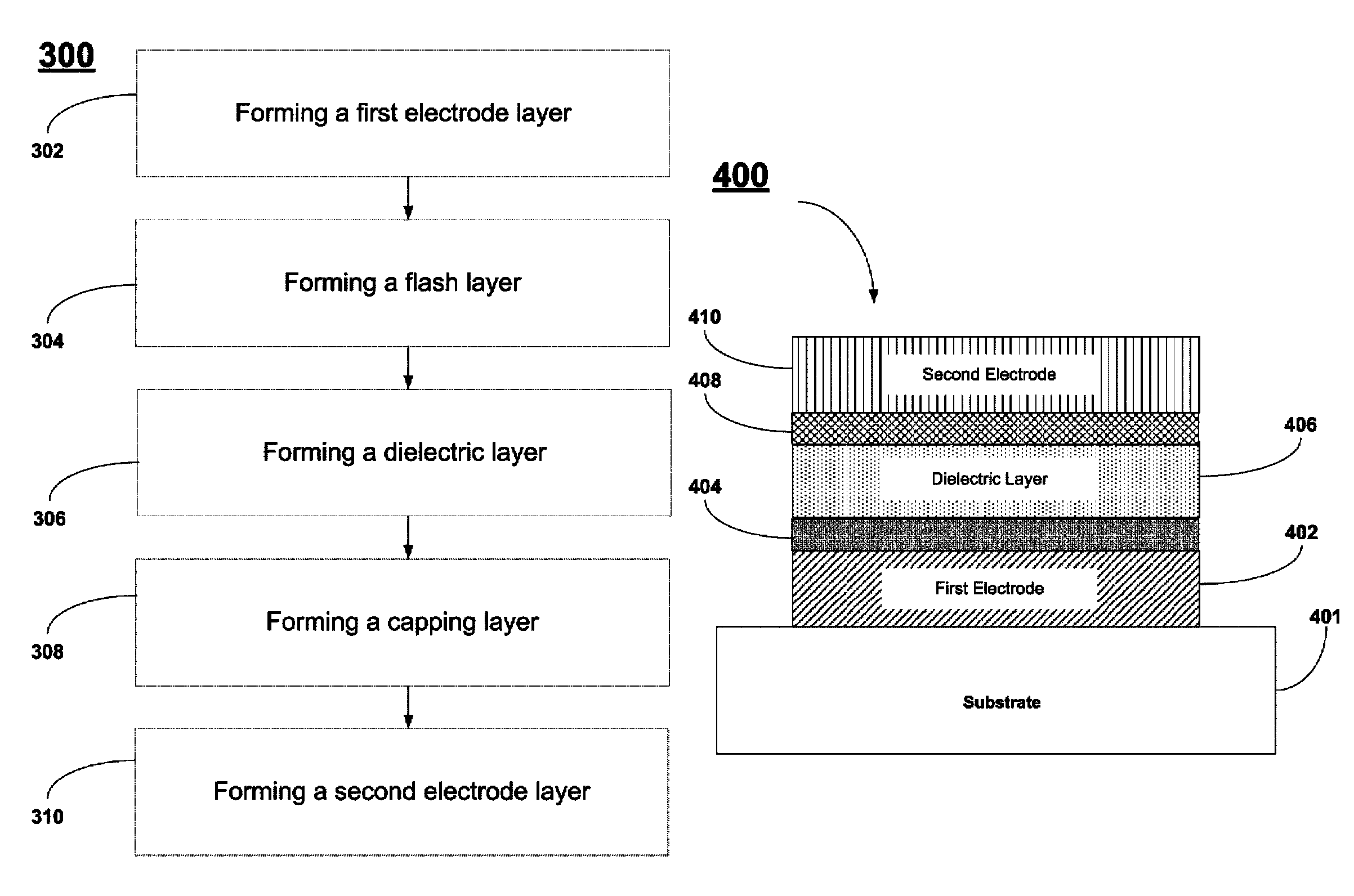
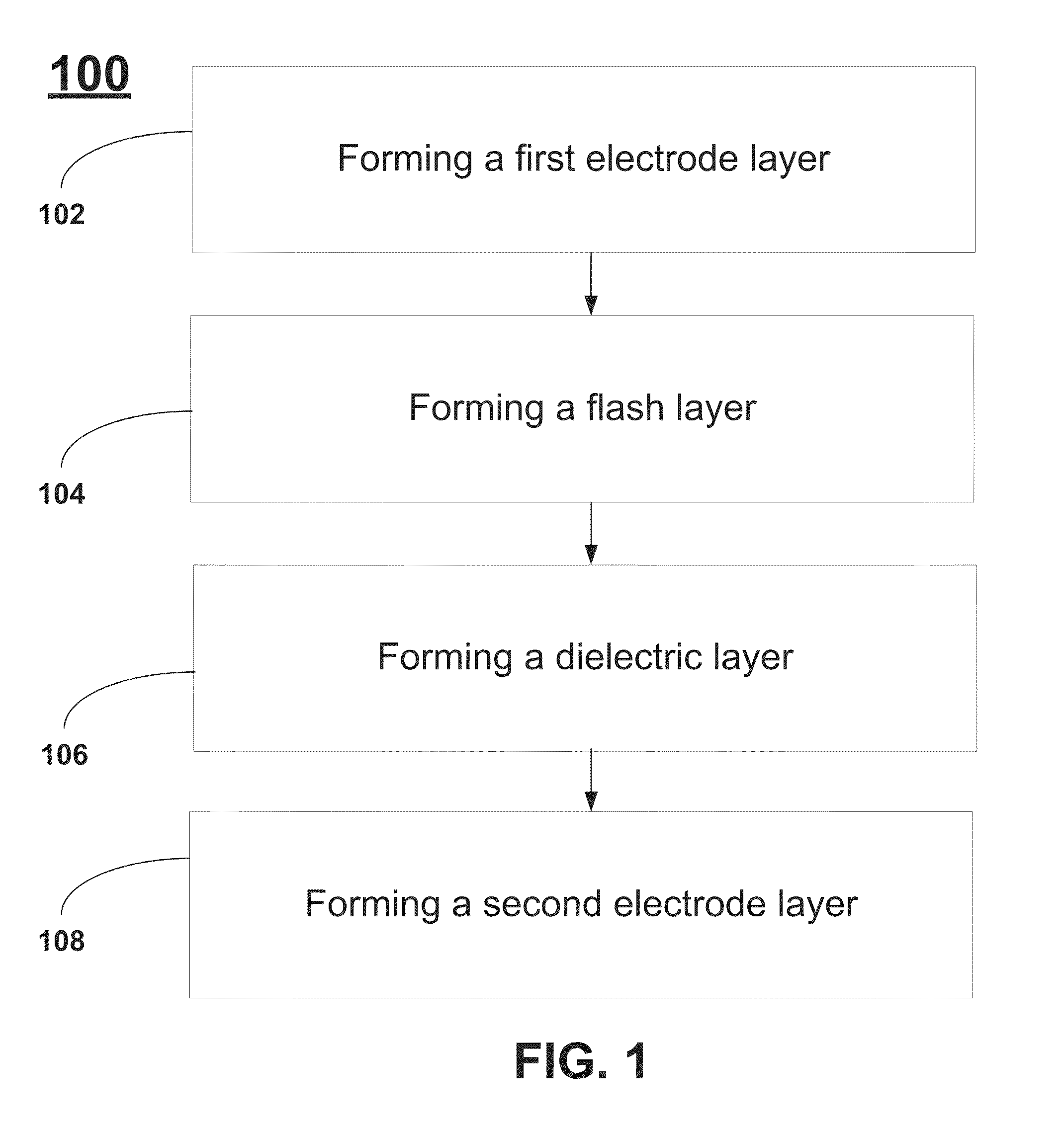
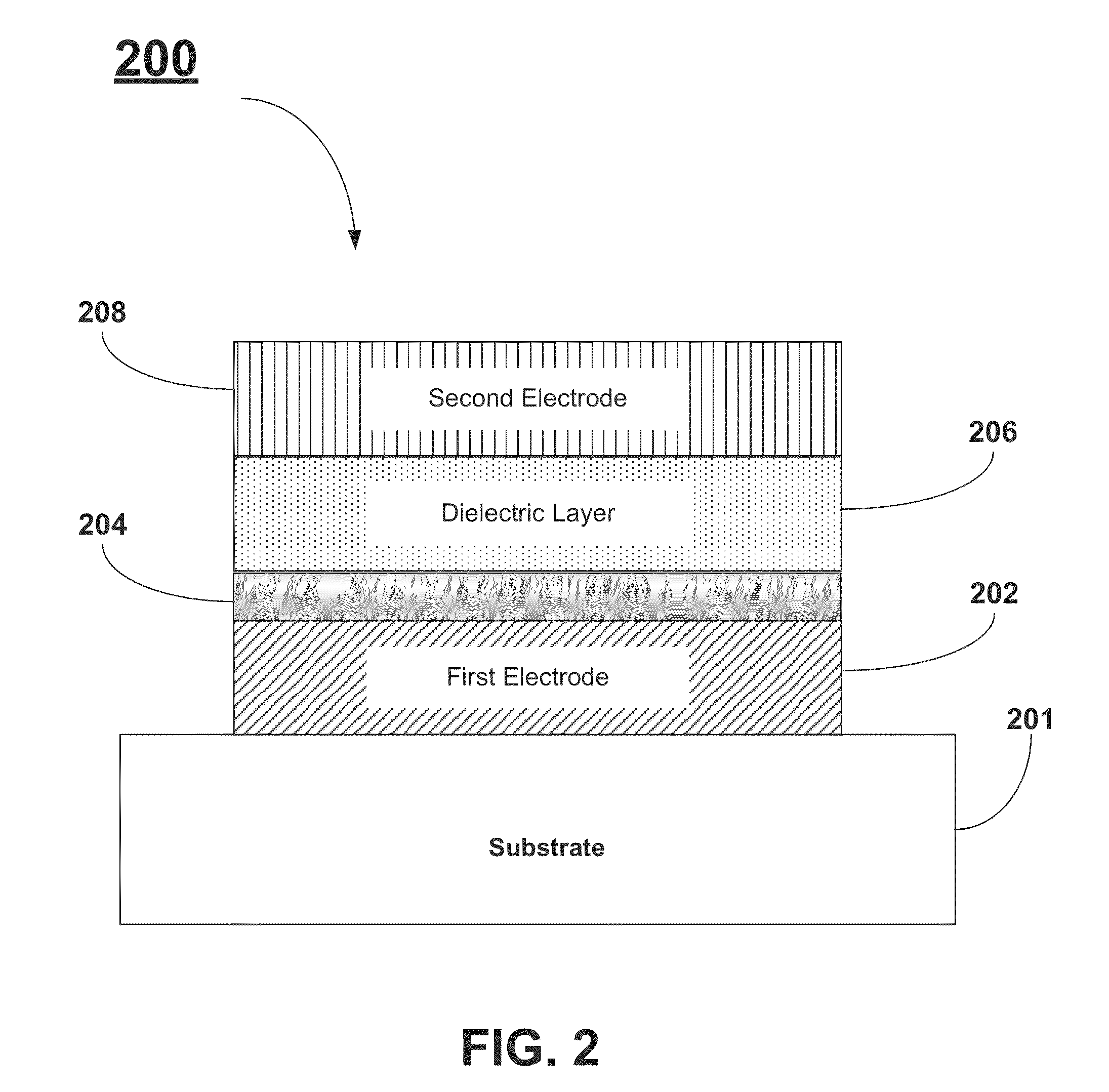
[0028]A detailed description of one or more embodiments is provided below along with accompanying figures. The detailed description is provided in connection with such embodiments, but is not limited to any particular example. The scope is limited only by the claims and numerous alternatives, modifications, and equivalents are encompassed. Numerous specific details are set forth in the following description in order to provide a thorough understanding. These details are provided for the purpose of example and the described techniques may be practiced according to the claims without some or all of these specific details. For the purpose of clarity, technical material that is known in the technical fields related to the embodiments has not been described in detail to avoid unnecessarily obscuring the description.

[0029]The mechanisms for charge transport discussed above suggest that there are several parameters that influence the leakage current across the metal-dielectric interface. E...


PUM

PropertyMeasurementUnit
cell capacitanceaaaaaaaaaa
physical thicknessaaaaaaaaaa

Abstract

A method for reducing the leakage current in DRAM Metal-Insulator-Metal capacitors includes forming a flash layer between the dielectric layer and the first electrode layer. A method for reducing the leakage current in DRAM Metal-Insulator-Metal capacitors includes forming a capping layer between the dielectric layer and the second electrode layer. The flash layer and the capping layer can be formed using an atomic layer deposition (ALD) technique. The precursor materials used for forming the flash layer and the capping layer are selected such they include at least one metal-oxygen bond. Additionally, the precursor materials are selected to also include “bulky” ligands.

Description

[0001]This document relates to the subject matter of a joint research agreement between Intermolecular, Inc. and Elpida Memory, Inc.FIELD OF THE DISCLOSURE[0002]The present disclosure relates generally to the field of dynamic random access memory (DRAM), and more particularly to methods of forming a capacitor stack for improved DRAM performance.BACKGROUND OF THE DISCLOSURE[0003]Dynamic Random Access Memory utilizes capacitors to store bits of information within an integrated circuit. A capacitor is formed by placing a dielectric material between two electrodes formed from conductive materials. A capacitor's ability to hold electrical charge (i.e., capacitance) is a function of the surface area of the capacitor plates A, the distance between the capacitor plates d, and the relative dielectric constant or k-value of the dielectric material. The capacitance is given by:[0004]C=κ⁢⁢ɛo⁢Ad(Eqn.⁢1)where ∈o represents the vacuum permittivity.[0005]The dielectric constant is a measure of a ma...

Claims


Application Information

Patent Timeline
Patent Type & Authority Patents(United States)
IPC IPC(8): H01L21/02H01G4/008H10N97/00
CPCH01L28/56H01L28/75H01L28/65
Inventor MALHOTRA, SANDRA G.ODE, HIROYUKIRUI, XIANGXIN
Owner INTERMOLECULAR
Learn More