Substrate processing apparatus, method of manufacturing semiconductor device and non-transitory computer-readable recording medium

a processing apparatus and semiconductor technology, applied in the direction of coatings, metallic material coating processes, chemical vapor deposition coatings, etc., can solve the problems of unintentional reaction in insufficient or satisfactorily performing the cleaning process on the exhaust buffer chamber, and the film has poor characteristics. , to achieve the effect of sharp increase in downtime and lowering the operation efficiency of the apparatus

Active Publication Date: 2015-05-12
KOKUSA ELECTRIC CO LTD
View PDF23 Cites 7 Cited by
  • Summary
  • Abstract
  • Description
  • Claims
  • Application Information

AI Technical Summary

Benefits of technology

[0013]To sufficiently perform a cleaning process on the inside of the exhaust buffer chamber, it is inferred that adhered materials may be removed by an operator's handwork during maintenance of an apparatus. However, in this case, a downtime sharply increases, thereby lowering operational efficiency of the apparatus. That is, it is difficult to conclude that a cleaning process may be satisfactorily performed on the inside of the exhaust buffer chamber.
[0014]It is a main object of the present invention to provide a substrate processing apparatus and a method of manufacturing a semiconductor device, which may sufficiently and satisfactorily perform a cleaning process on the inside of an exhaust buffer chamber even if a gas exhaust process is performed using the exhaust buffer chamber.

Problems solved by technology

However, according to the above-described conventional arts, a cleaning process may not be sufficiently or satisfactorily performed on an exhaust buffer chamber.
In this case, there may be cases in which any one gas remains in the exhaust buffer chamber to cause an unintentional reaction in the exhaust buffer chamber.
In particular, since the inside of the exhaust buffer chamber is not under temperature or pressure conditions for forming a good film unlike the inside of the processing space, a film having poor characteristics (i.e., a film having a deviation in film density or film thickness) is formed.
Since the poor film is easily delaminated due to a pressure variation during a switch of the supply of gases, the delaminated film may intrude into the processing space, adversely affect characteristics of a film formed on the substrate, and cause a reduction in yield.
However, since an active cleaning gas is deactivated in the processing space before the active cleaning gas reaches the exhaust buffer chamber, the inside of the exhaust buffer chamber may not be sufficiently cleaned.
Also, even if the cleaning gas is directly supplied into an exhaust pipe, the exhaust buffer chamber disposed at an upstream side of the exhaust pipe may not be sufficiently cleaned.
However, in this case, a downtime sharply increases, thereby lowering operational efficiency of the apparatus.
That is, it is difficult to conclude that a cleaning process may be satisfactorily performed on the inside of the exhaust buffer chamber.

Method used


Image

  • Substrate processing apparatus, method of manufacturing semiconductor device and non-transitory computer-readable recording medium
  • Substrate processing apparatus, method of manufacturing semiconductor device and non-transitory computer-readable recording medium
  • Substrate processing apparatus, method of manufacturing semiconductor device and non-transitory computer-readable recording medium

Examples


Embodiment Construction

One Embodiment of the Present Invention

[0023]One embodiment of the present invention will now be described with reference to the accompanying drawings.

(1) Structure of Substrate Processing Apparatus

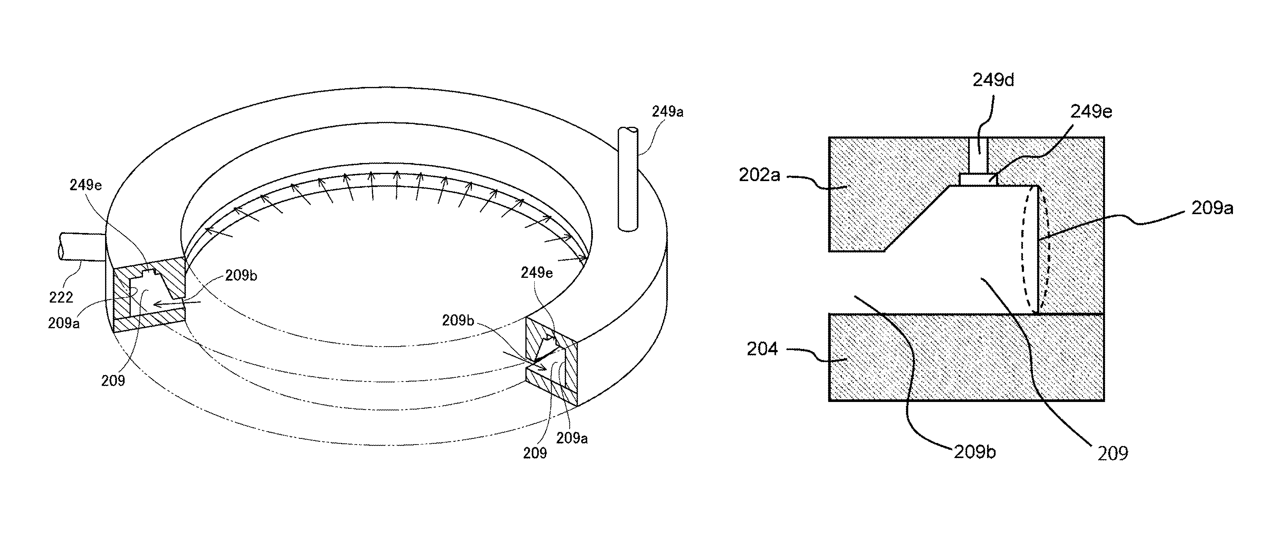
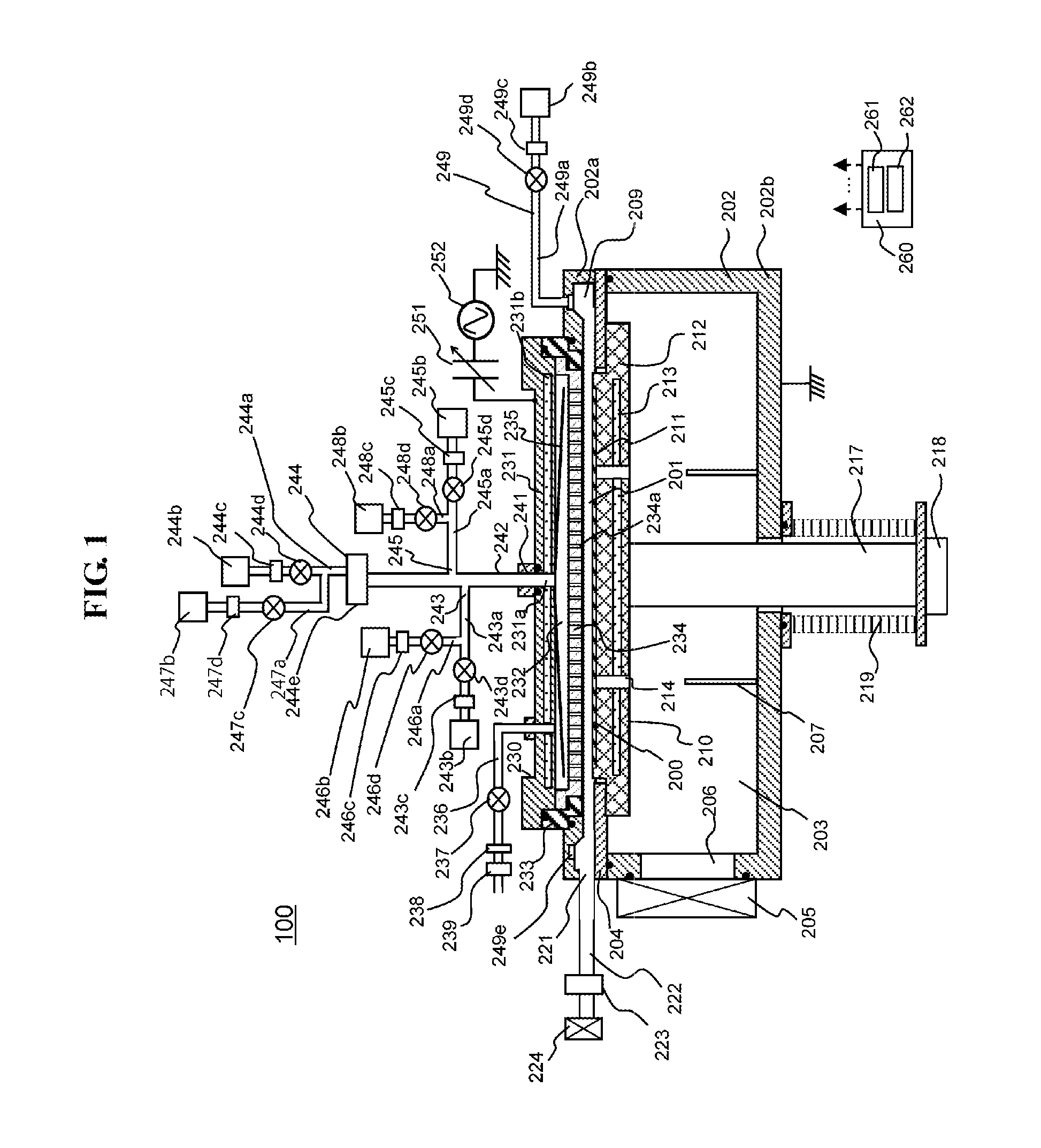
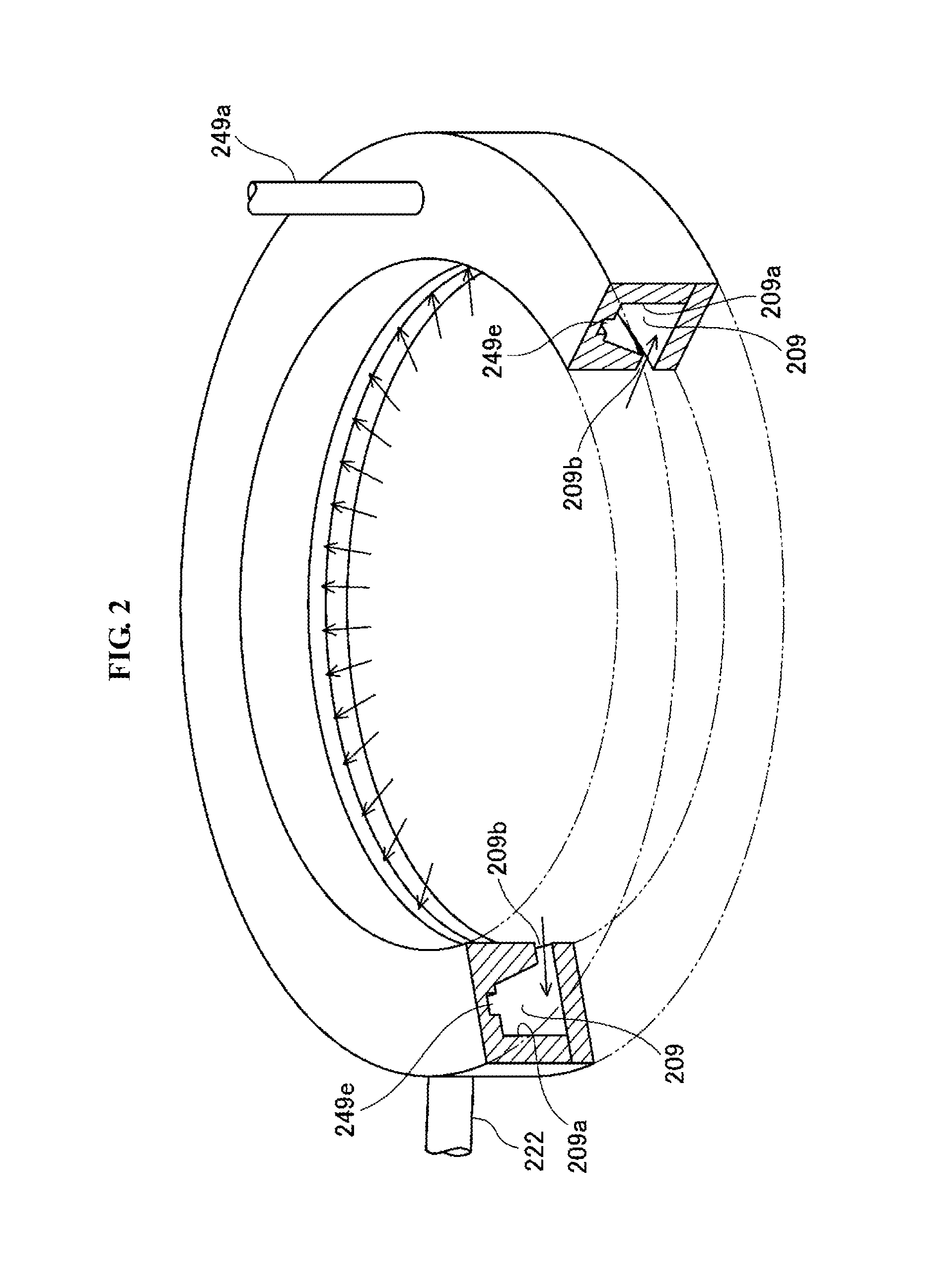
[0024]A substrate processing apparatus according to the present embodiment is configured as a single-wafer-type substrate processing apparatus for processing substrates serving as processing objects one by one. As the substrates serving as the processing objects, for example, there may be a semiconductor wafer substrate (hereinafter, referred to simply as a “wafer”) on which a semiconductor device is manufactured. Although processes performed on a substrate may include an etching process, an ashing process and a film forming process, particularly, the film forming process will be described in the present embodiment. As a typical example of the film forming process, there is an alternate supply process.

[0025]Hereinafter, a structure of a substrate processing apparatus according to the pres...


PUM


Abstract

Provided are a substrate processing apparatus and a method of manufacturing a semiconductor device, which perform a cleaning process on the inside of an exhaust buffer chamber even if gases are exhausted using the exhaust buffer chamber. The substrate processing apparatus includes a processing space to process a substrate on a substrate placing surface, a gas supply system to supply gases into the processing space through a side facing the substrate placing surface, an exhaust buffer chamber including a communication hole communicating with the processing space at least at a side portion of the processing space and a gas flow blocking wall extending in a blocking direction of the gases flowing through the communication hole, a gas exhaust system configured to exhaust the gases supplied into the exhaust buffer chamber, and a cleaning gas supply pipe configured to supply a cleaning gas into the exhaust buffer chamber.

Description

CROSS-REFERENCE TO RELATED PATENT APPLICATION[0001]This U.S. non-provisional patent application claims priority under 35 U.S.C. §119 of Japanese Patent Application No. 2014-063076, filed on Mar. 26, 2014, in the Japanese Patent Office, the entire contents of which are hereby incorporated by reference.BACKGROUND OF THE INVENTION[0002]1. Field of the Invention[0003]The present invention relates to a substrate processing apparatus, a method of manufacturing a semiconductor device and a non-transitory computer-readable recording medium.[0004]2. Description of the Related Art[0005]In general, a substrate processing apparatus for performing processes (e.g., a film forming process) on a substrate (e.g., a wafer) is used in a process of manufacturing a semiconductor device. With the scaling-up of a substrate or an increase in the precision of processes, a single-wafer-type substrate processing apparatus configured to process substrates one by one has widely been used as the substrate proces...

Claims


Application Information

Patent Timeline
Patent Type & Authority Patents(United States)
IPC IPC(8): C23C16/44C23C16/458H01L21/00C23C16/52H01L21/02
CPCC23C16/4405C23C16/4586C23C16/52C23C16/4412H01L21/02104C23C16/45523H01L21/0217H01L21/0228
Inventor KAMAKURA, TSUKASAKAMEDA, KENJI
Owner KOKUSA ELECTRIC CO LTD
Why Eureka
Try Eureka