Organic electroluminescence element

an electroluminescent element and organic technology, applied in the direction of organic semiconductor devices, thermoelectric devices, solid-state devices, etc., can solve the problems of increasing the difficulty of mask position adjustment, increasing the difficulty of mask positioning adjustment, and extremely difficult application thereof, so as to improve the light emission efficiency and low-voltage drive characteristics of application-type organic el elements, and enhance the longevity

Inactive Publication Date: 2015-05-12
JOLED INC
View PDF154 Cites 17 Cited by
  • Summary
  • Abstract
  • Description
  • Claims
  • Application Information

AI Technical Summary

Benefits of technology

[0019]However, although application-type organic EL elements have such advantageous features as described above, there is a demand to improve application-type organic EL elements so as to further enhance low-voltage drive characteristics and light emitting efficiency of application-type organic EL elements. In particular, in the manufacturing of application-type organic EL elements, there is a demand to further improve hole injection efficiency of application-type organic EL elements and to provide application-type organic EL elements with a further enhanced level of longevity.
[0022]In the organic EL element pertaining to one aspect of the present invention, the hole injection layer contains tungsten oxide. Further, the hole injection layer has, in an electronic state thereof, an occupied energy level which is 1.8 eV to 3.6 eV lower than the lowest energy level of a valence band of the hole injection layer, in terms of binding energy. By the hole injection layer having such an occupied energy level, the hole injection barrier between the hole injection layer and the functional layer is suppressed to a low level. Resultantly, the organic EL element pertaining to one aspect of the present invention has excellent hole injection efficiency, can be driven at a low voltage, and is expected to exhibit excellent light-emitting efficiency.
[0024]In view of such problems, in the organic EL element pertaining to one aspect of the present invention, the hole injection layer has a recessed structure such that a portion of a surface thereof facing the functional layer is closer to the anode than other portions of the surface facing the functional layer. In addition, in the organic EL element pertaining to one aspect of the present invention, an inner surface (an inner bottom surface and an inner side surface) of a recessed portion of the hole injection layer is in contact with the functional layer. Due to this, the wettability of the functional layer with respect to the hole injection layer is improved. As such, even when the film thickness reduction of the hole injection layer occurs, material for forming the functional layer is prevented from being applied ununiformly, and accordingly, an organic EL element having excellent characteristics is formed by patterning being performed with high precision. As a result, the risk of the light-emitting characteristics of the organic EL element being affected can be reduced preemptively by preventing problems such as ununiform luminous intensity and reduction in life-span from occurring.

Problems solved by technology

However, although vapor deposition-type organic EL elements may be ideal for use in small-sized organic EL panels, application thereof is extremely difficult, for example, to full-color, large-sized organic EL panels having display sizes of around 100 inches.
The difficulty of such an application derives from the technology applied in the manufacturing of a vapor deposition-type organic EL element.
However, as the surface area of the organic EL panel to be manufactured becomes larger, it becomes more and more difficult to maintain the precision with which mask position adjustment is performed.
Hence, the manufacturing of a large-sized display without any deficiencies is extremely difficult when applying vapor deposition-type organic EL elements.

Method used


Image

  • Organic electroluminescence element
  • Organic electroluminescence element
  • Organic electroluminescence element

Examples


embodiment 2

[0218]As such, the inventors arrived at a structure of an organic EL element where, within an area of the hole injection layer defined by banks, a surface of the hole injection layer facing the functional layer has a recessed structure, and further, the recessed structure has a recessed portion whose inner surface is in contact with the functional layer, as description is provided in embodiment 2 of the present disclosure presented in the following.

embodiment 1

[0219]In the following, description is provided on another embodiment of the present disclosure while focusing on aspects differing from

[0220]

[0221](Overall Structure of Light-Emitting Element)

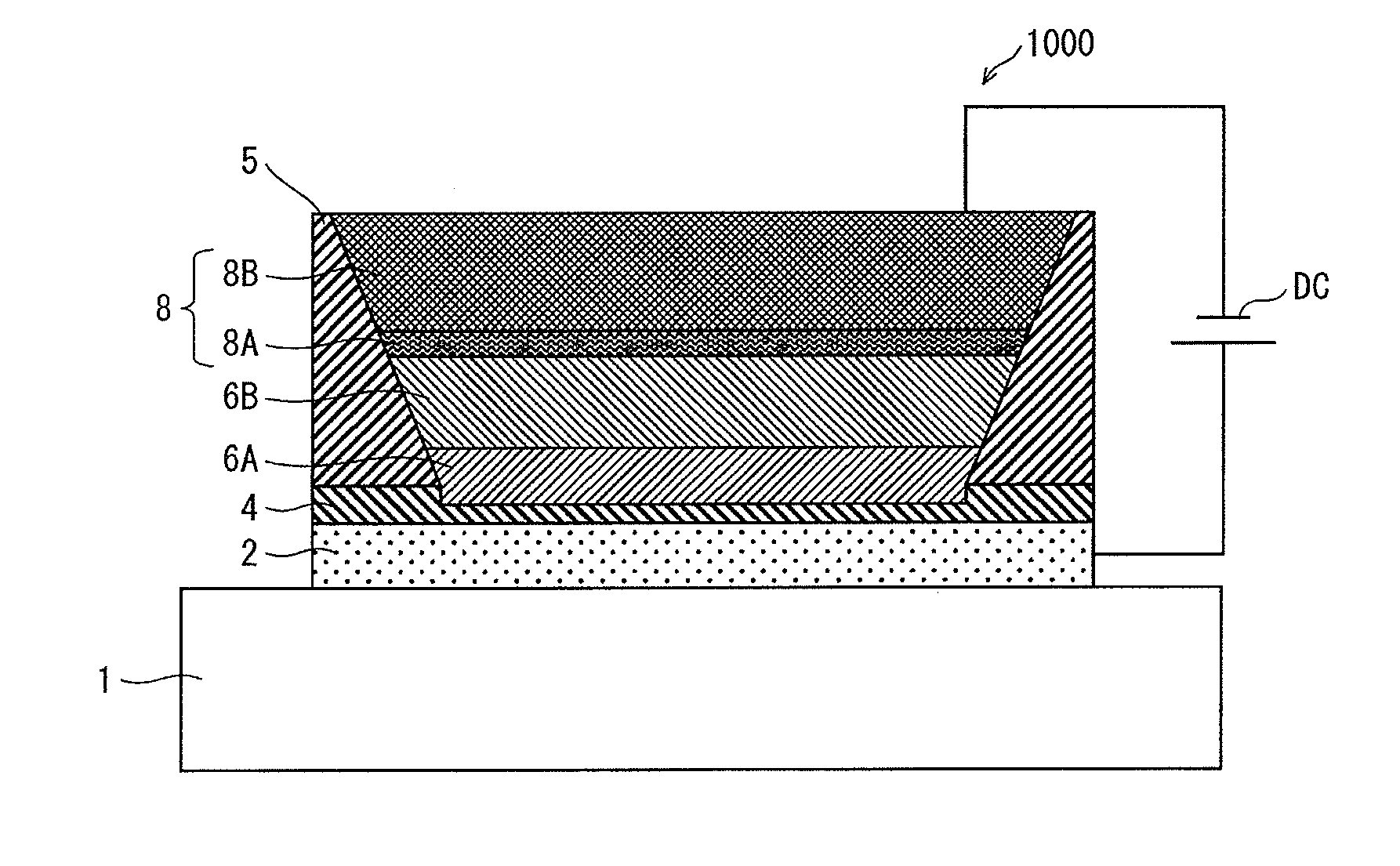
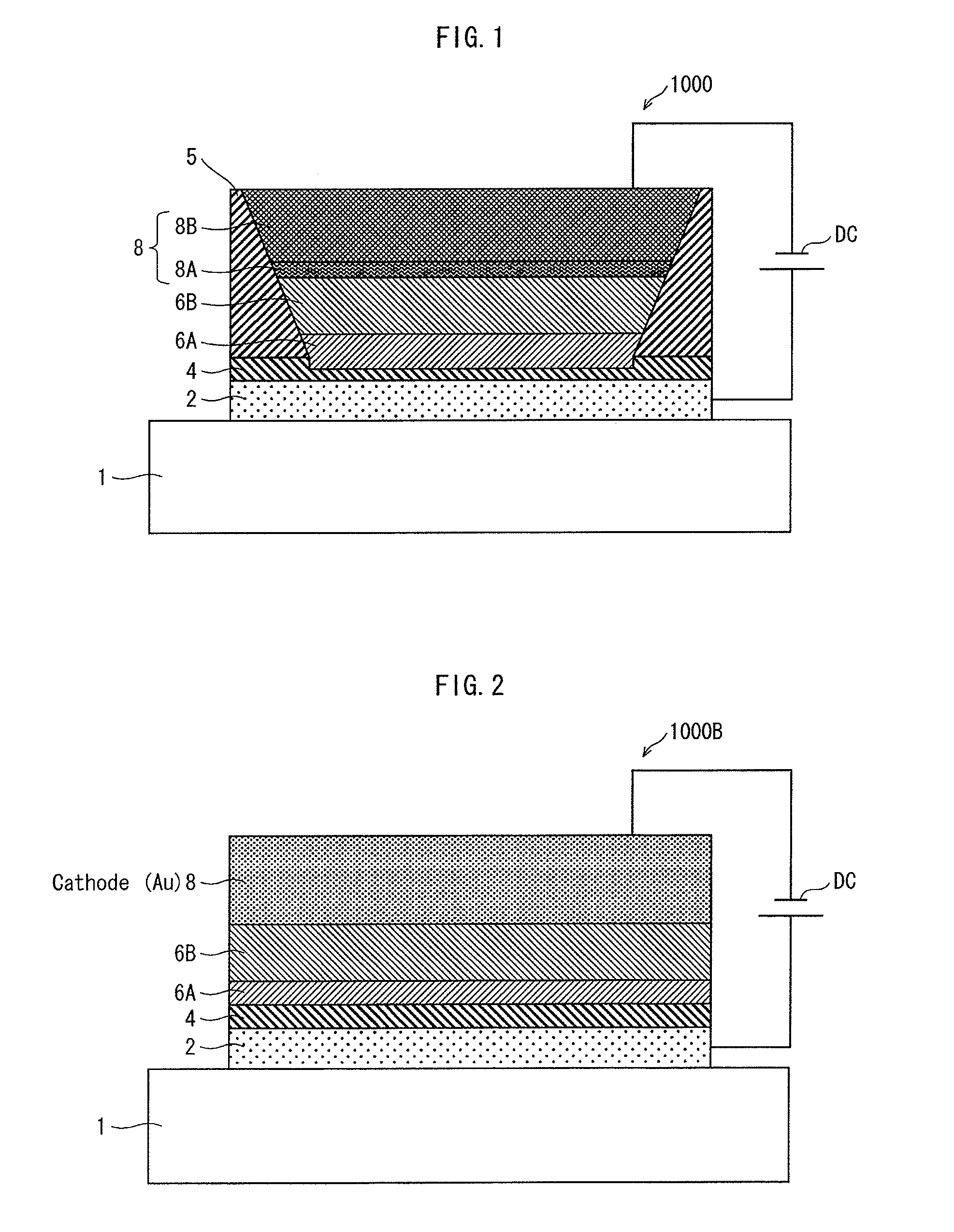
[0222]FIG. 16 is a schematic view illustrating a layered state of layers of a light-emitting element 1000C pertaining to embodiment 2. FIG. 17 is an enlarged view of a part surrounded by dashed-dotted lines in FIG. 16.

[0223]As illustrated in FIG. 16, the light-emitting element 1000C is a top emission type organic light-emitting element in which pixels corresponding to the colors R, G, and B are arranged so as to form lines or to form a matrix. Further, each pixel has a layered structure where various layers are layered above the substrate 1.

[0224]The light-emitting element 1000C differs from the organic EL element 1000 in embodiment 1 in that, in the light-emitting element 1000C, the hole injection layer 4 is disposed on an upper surface of an anode (the anode 2) with an ITO layer 3 interposed...

embodiment 5

[0285]FIG. 28 is a perspective view illustrating a display apparatus pertaining to embodiment 5 and the like. As illustrated in FIG. 28, a display apparatus 300 pertaining to one aspect of the present invention is an organic EL display formed by a plurality of pixels arranged in a matrix extending in both the row direction and the column direction. Each pixel emits light of a corresponding color among the colors of R, G, and B and is composed of the light-emitting element pertaining to one aspect of the present invention.

[0286](Modification)

[0287]Up to this point, specific explanation has been provided of the light-emitting element, the display apparatus, and the manufacturing method of the light-emitting element, each of which pertaining to one aspect of the present invention. However, it should be noted that the above-described description provided in the embodiments of the light-emitting element, the display apparatus, and the manufacturing method of the light-emitting element, e...


PUM


Abstract

An organic light-emitting element comprising: an anode; a cathode; banks; a functional layer between the anode and the cathode; and a hole injection layer between the anode and the functional layer. The functional layer includes one or more sublayers including a light-emitting sublayer defined by the banks and that contains an organic material. The hole injection layer comprises tungsten oxide, includes an occupied energy level that is approximately 1.8 electron volts to approximately 3.6 electron volts lower than a lowest energy level of a valence band of the hole injection layer in terms of a binding energy, has a surface facing the functional layer, and has a recessed structure such that a portion of the surface overlapping with the light-emitting sublayer is located closer to the anode than other portions. The recessed structure has a recessed portion whose inner surface is in contact with the functional layer.

Description

CROSS REFERENCE TO RELATED APPLICATION[0001]This is a continuation application of PCT Application No. PCT / JP2010 / 004993 filed Aug. 6, 2010, designating the United States of America, the disclosure of which, including the specification, drawings and claims, is incorporated herein by reference in its entirety.TECHNICAL FIELD[0002]The present disclosure relates to an organic electric-field light-emitting element (referred to hereinafter as an “organic EL element”), which is an electric light-emitting element. Particularly, the present disclosure relates to a technology for driving such an organic EL element at low electricity while ensuring a wide range of luminous intensity from low luminous intensity to high luminous intensity for the use as a light source or the like.DESCRIPTION OF THE RELATED ART[0003]In recent years, progress is being made in research and development of diverse functional elements which involve the use of an organic semiconductor.[0004]Organic EL elements are know...

Claims


Application Information

Patent Timeline
Patent Type & Authority Patents(United States)
IPC IPC(8): H01L51/50H01L51/52
CPCH01L51/5088H01L51/5209H01L51/5218H01L2251/5369H10K50/17H10K50/813H10K50/818H10K2102/331
Inventor HARADA, KENJINISHIYAMA, SEIJIKOMATSU, TAKAHIROTAKEUCHI, TAKAYUKIOHUCHI, SATORUTSUKAMOTO, YOSHIAKIFUJIMURA, SHINYASAKANOUE, KEI
Owner JOLED INC
Why Eureka
Try Eureka