TCCT match circuit for plasma etch chambers

a match circuit and plasma etching technology, applied in the field of semiconductor fabrication, can solve the problems of limited tct range, limited transformer coupled plasma power, and existing transformer coupled capacitive tuning (tcct) match designs

Active Publication Date: 2015-06-16
LAM RES CORP
View PDF11 Cites 26 Cited by
  • Summary
  • Abstract
  • Description
  • Claims
  • Application Information

AI Technical Summary

Problems solved by technology

Existing transformer coupled capacitive tuning (TCCT) match designs suffer from a number of problems, especially when utilized to perform manufacturing processes for magneto-resistive random access memory (MRAM).
Problems include a limited TCCT range, limited transformer coupled plasma (TCP) power, high coil voltages, and coil arcing.
As a result, the process window of the reactor chamber can be quite limited, meaning that a variety of recipes cannot be accommodated.
If a recipe out of the process window is forced to run, it may be aborted due to over voltage and / or over current interlocks, and even worse, may result in arcing of the TPC coil and destruction of the ceramic window and ceramic cross.
Furthermore, a sputtering effect of the ceramic window due to capacitive coupling by the TCP coil can develop over time when terminal voltages are not well balanced.
The result is sputtering of particles from the ceramic window that are subsequently deposited on the wafer, which may result in loss of yield.
This effect can limit the operational longevity of the reactor to, for example, 500 RF hours of operation.

Method used


Image

  • TCCT match circuit for plasma etch chambers
  • TCCT match circuit for plasma etch chambers
  • TCCT match circuit for plasma etch chambers

Examples


Embodiment Construction

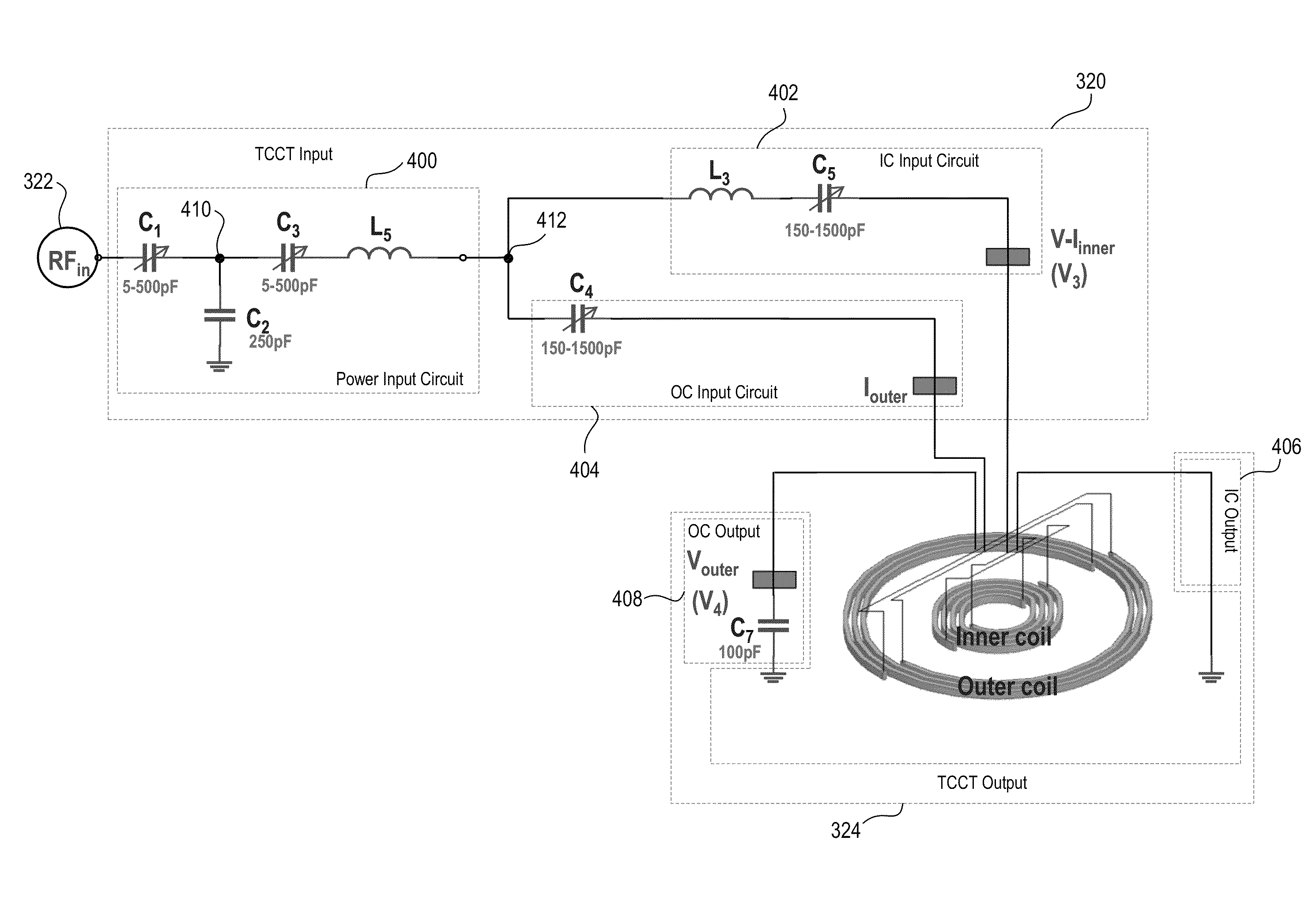
[0031]Disclosed is a TCCT match circuit for use in etching semiconductor substrates and layers formed thereon during the manufacture of semiconductor devices. The The TCCT match circuitry controls the operation of a TCP coil disposed over a dielectric window of a chamber in which etching is performed.

[0032]In the following description, numerous specific details are set forth in order to provide a thorough understanding of the present invention. However, it will be apparent to one skilled in the art that the present invention may be practiced without some of these specific details. In other instances, well known process operations and implementation details have not been described in detail in order to avoid unnecessarily obscuring the invention.

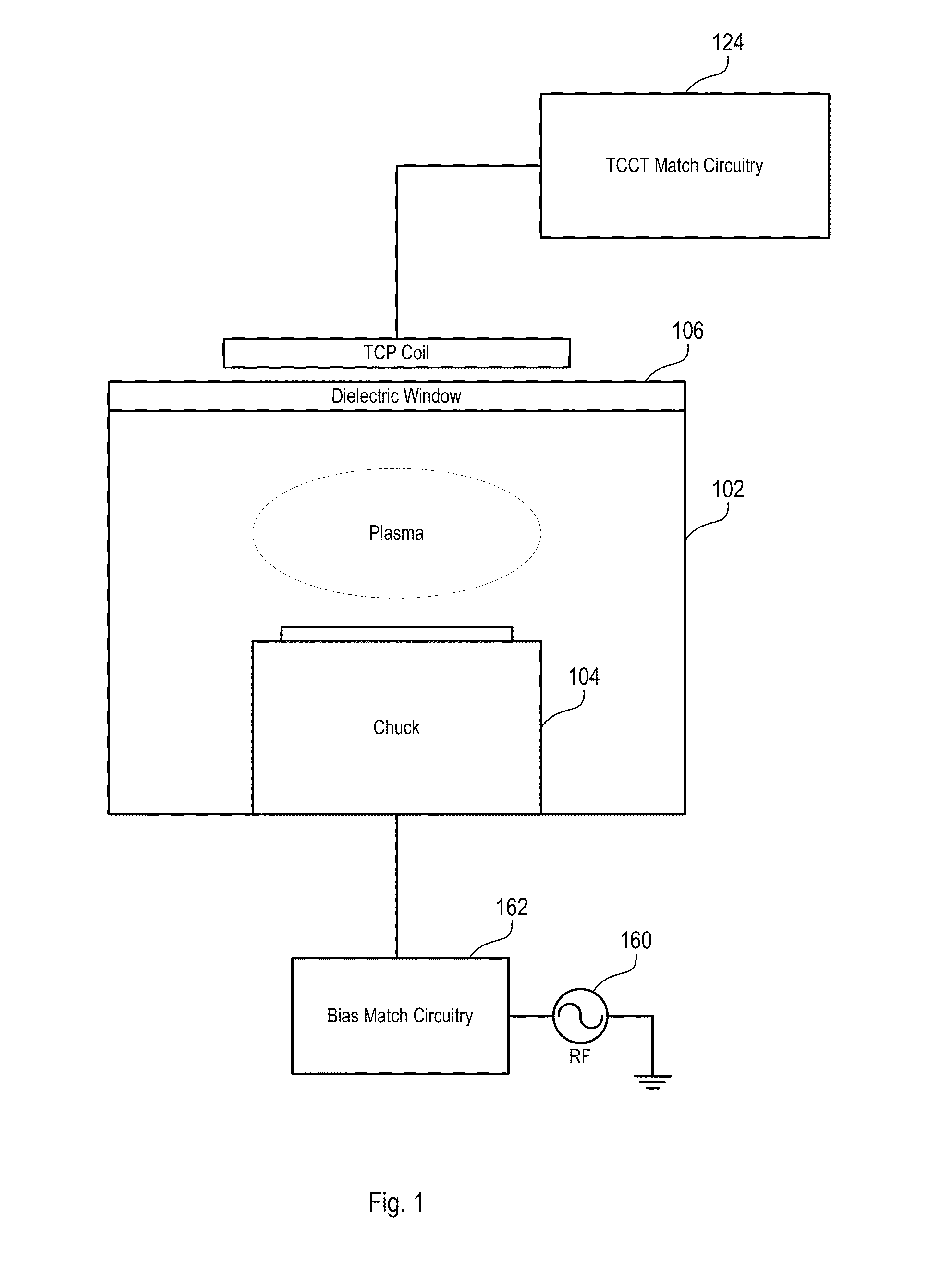
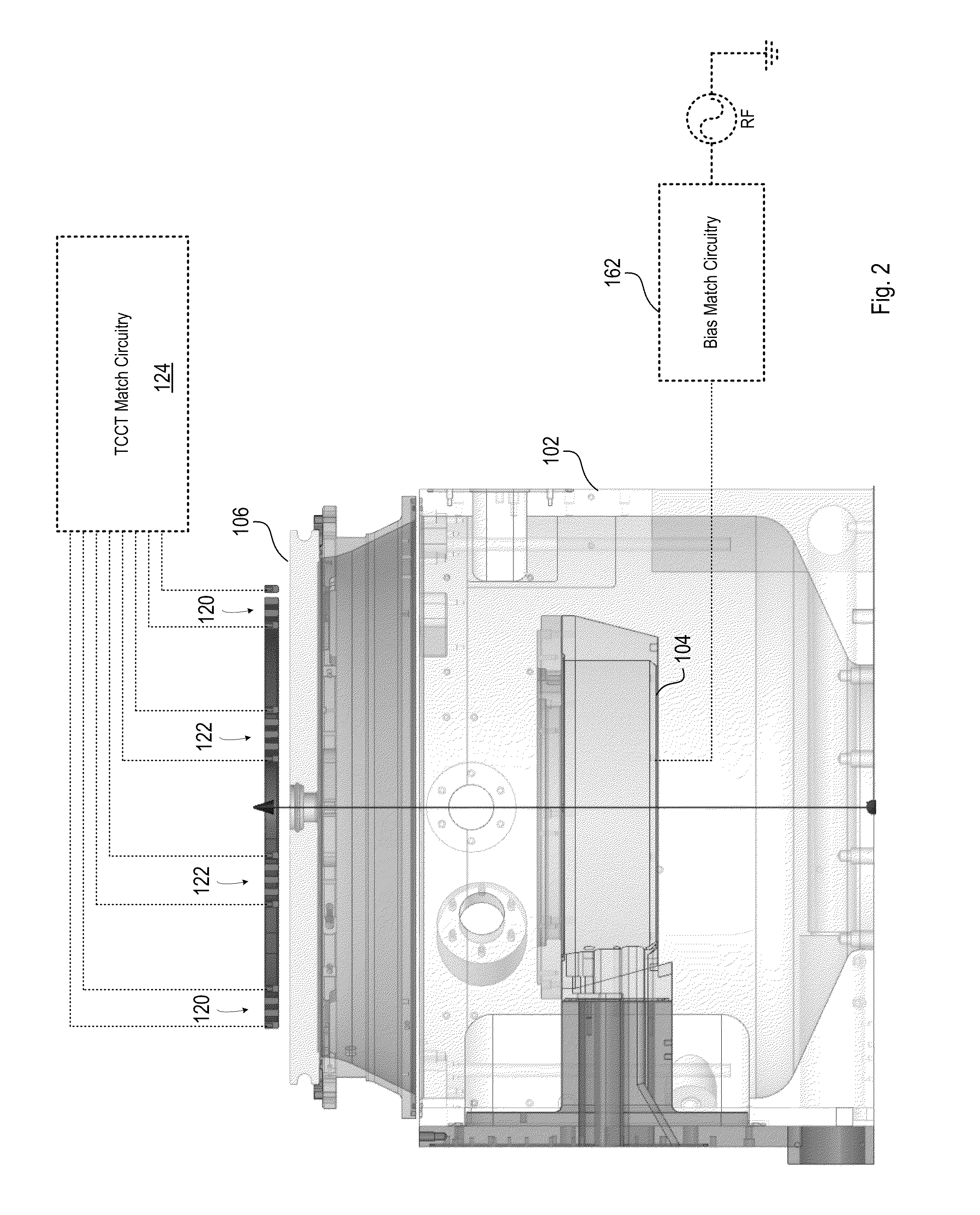
[0033]FIG. 1 illustrates a plasma processing system utilized for etching operations, in accordance with one embodiment of the present invention. The system includes a chamber 102 that includes a chuck 104, and a dielectric window 106. The chu...


PUM


Abstract

A match circuit includes the following: a power input circuit coupled to an RF source; an inner coil input circuit coupled between the power input circuit and an input terminal of an inner coil, the inner coil input circuit including an inductor and a capacitor coupled in series to the inductor, the inductor connecting to the power input circuit, and the capacitor connecting to the input terminal of the inner coil, a first node being defined between the power input circuit and the inner coil input circuit; an inner coil output circuit coupled between an output terminal of the inner coil and ground, the inner coil output circuit defining a direct pass-through connection to ground; an outer coil input circuit coupled between the first node and an input terminal of an outer coil; and an outer coil output circuit coupled between an output terminal of the outer coil and ground.

Description

CLAIM OF PRIORITY[0001]This application claims priority to U.S. Provisional Application No. 61 / 747,919, filed on Dec. 31, 2012, and entitled “TCCT Match Circuit for Plasma Etch Chambers.” This application claims priority as a Continuation-in-Part of U.S. patent application Ser. No. 13 / 658,652, filed on Oct. 23, 2012, and entitled “Faraday Shield Having Plasma Density Decoupling Structure Between TCP Coiling Zones,” which claims priority as a Continuation-in-Part of U.S. patent application Ser. No. 13 / 198,683, filed on Aug. 4, 2011, and entitled “Internal Faraday Shield Having Distributed Chevron Patterns and Correlated Positioning Relative to External Inner and Outer TCP Coil, which claims priority to U.S. Provisional Patent Application No. 61 / 480,314 filed on Apr. 28, 2011 and entitled “Internal Faraday Shield Having Distributed Chevron Patterns and Correlated Positioning Relative to External Inner and outer TCP Coil.” The disclosures of these applications are incorporated herein b...

Claims


Application Information

Patent Timeline
Patent Type & Authority Patents(United States)
IPC IPC(8): H03H7/38H03H7/40
CPCH03H7/38H03H7/40
Inventor LONG, MAOLINMARSH, RICKYPATERSON, ALEX
Owner LAM RES CORP
Why Eureka
Try Eureka