Method for generating a topography of an FDSOI integrated circuit

Active Publication Date: 2015-07-28
STMICROELECTRONICS SRL
View PDF3 Cites 7 Cited by
  • Summary
  • Abstract
  • Description
  • Claims
  • Application Information

AI Technical Summary

Benefits of technology

[0047]the second cell includes a diode protecting against antenna effects or a well tap cell, said second cell comprising a P-type doping well arranged in the alignment of the P-type well of the pMOS transistor and comprising an N-type doping well arranged in the alignment of the N-type well of the nMOS transistor, the second cell comprising a lower metal connection element coupled to its P-type doping well and coupled to a higher-level metal connec

Problems solved by technology

Thus, the doping level of the channel of the transistors cannot therefore reveal substantial variations, which prevents the threshold voltages from being differentiated in this way.
However, the practical implementation of an integrated circuit of this type proves technically challenging and economically prohibitive.
A practical problem that arises with any technological development relating to circuits of this type is that existing design tools may prove to be incompatible or may require substantial computing developments.
Large circuits are in fact too complex to be designed manually and require appropriate computing tools, notably to avoid the risks of design errors.
The algorithmic synthesis is not necessarily enough to guarantee the absence

Method used


Image

  • Method for generating a topography of an FDSOI integrated circuit
  • Method for generating a topography of an FDSOI integrated circuit
  • Method for generating a topography of an FDSOI integrated circuit

Examples


Embodiment Construction

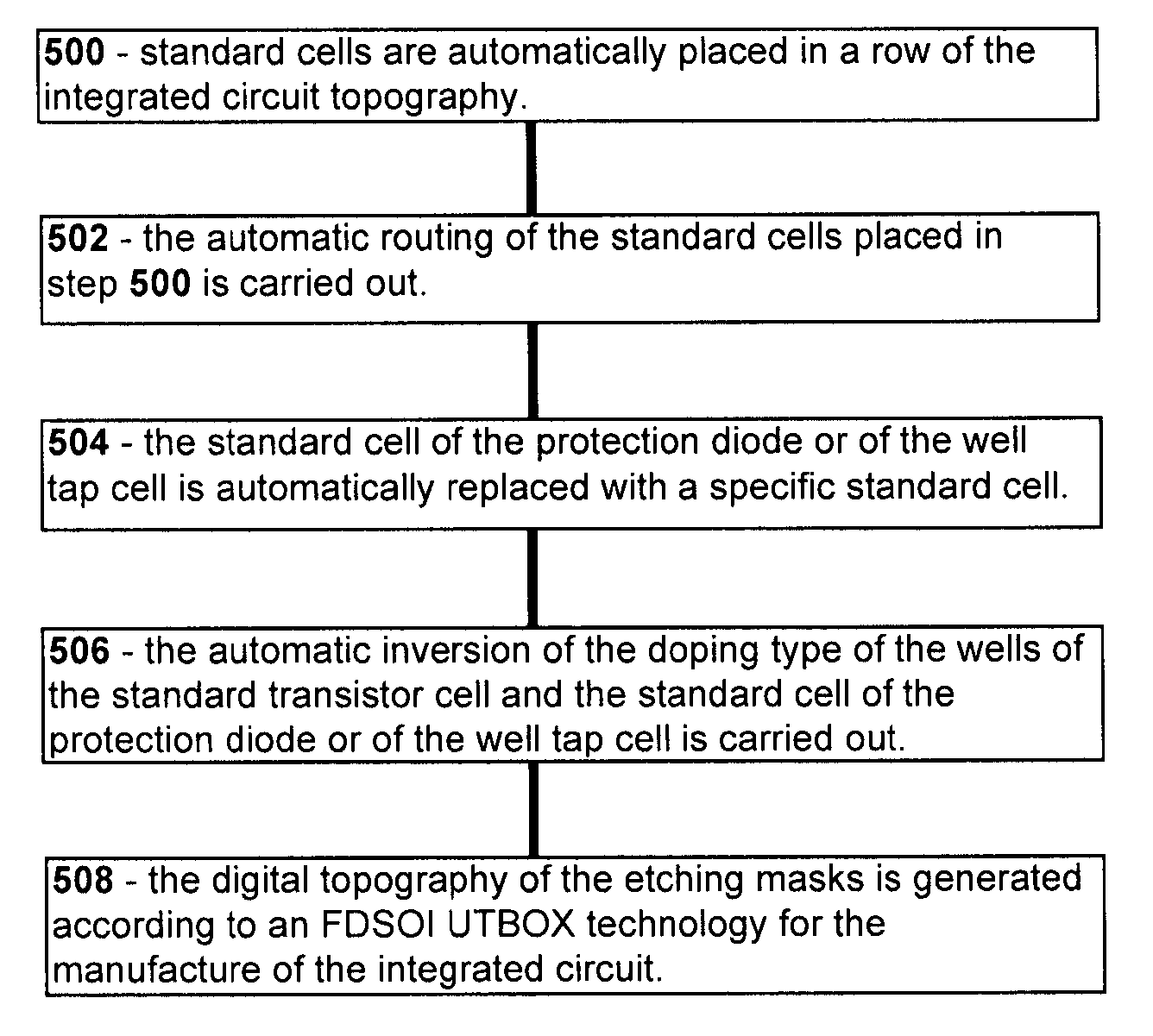
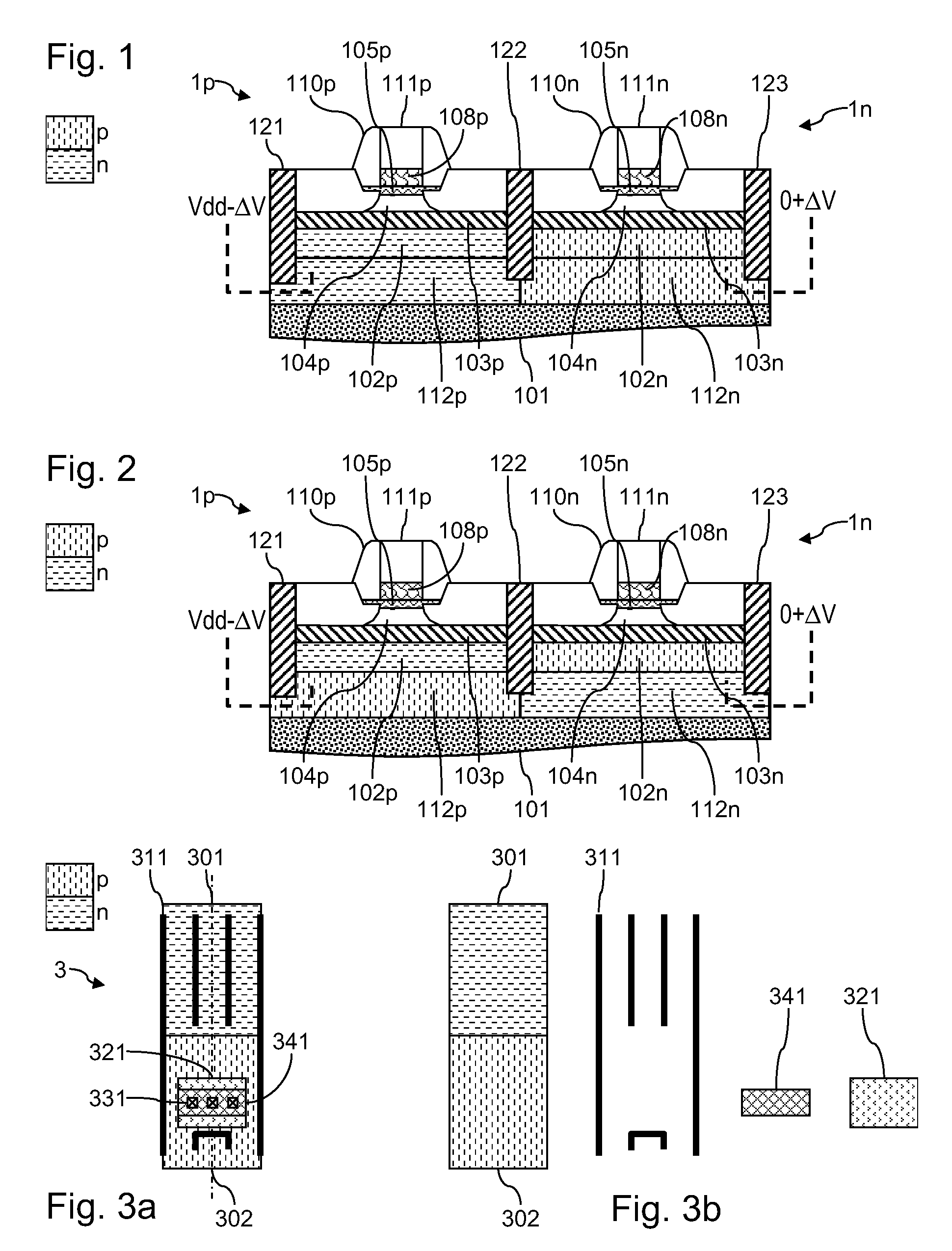
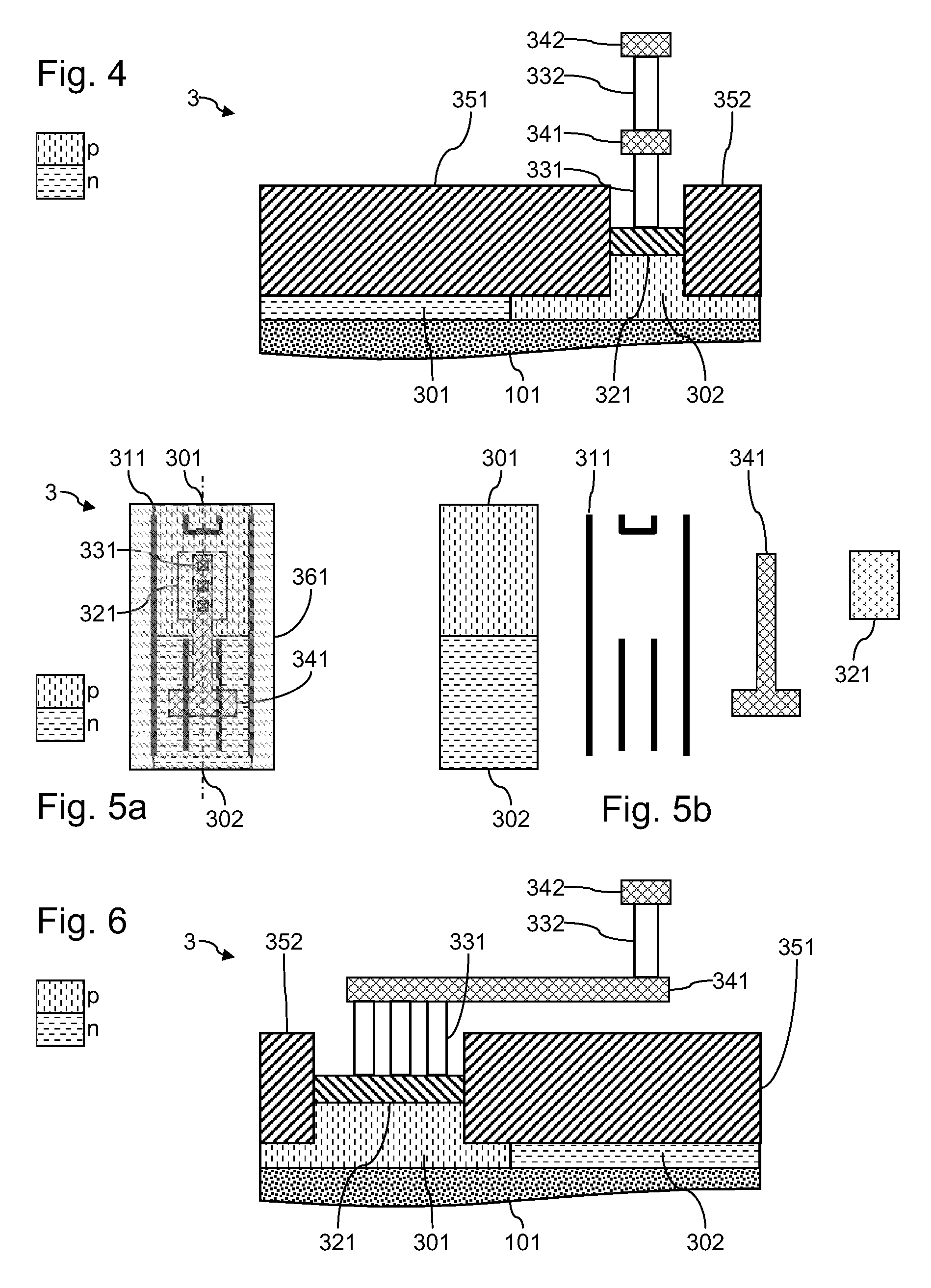
[0063]In the context of the design of FDSOI-UTBOX integrated circuits with an FBB type biasing, the invention aims to simplify the generation of a topography of masks when nMOS transistors are intended to overhang an N-type well and when pMOS transistors are intended to overhang a P-type well. The invention proposes to replace standard cells of well tap cells or of diodes protecting against antenna effects with newly defined standard cells, before proceeding with an inversion of the doping types of a set of wells. In these new standard cells, a metal connection element extends on either side of the axis of a row of cells, i.e. plumb with both the N-type well and the P-type well of the standard cell. The metal connection element is interconnected to an N-type well before the inversion of the doping types.

[0064]The performance of a place and route step after the inversion of the doping types of the wells can thus be avoided. In fact, once the routing has been carried out with a first ...


PUM


Abstract

An IC including first and second FDSOI UTBOX cells arranged in a row, the first having an nMOS transistor arranged plumb with and above a ground plane and an N-type well, and a pMOS transistor arranged plumb with and above a ground plane and a P-type well, the N-type well and the P-type well being arranged on either side of a row axis, wherein the second includes a diode protecting against antenna effects or a well tap cell, the second cell comprising a P-type well arranged in the alignment of the P-type well of the pMOS transistor and comprising an N-type well arranged in the alignment of the N-type well of the nMOS transistor, the second cell comprising a metal connection coupled to its P-type well and coupled to a higher-level metal connection element arranged plumb with the N-type well, the metal connection extending on either side of the axis.

Description

RELATED APPLICATIONS[0001]Under 35 USC 119, this application claims the benefit of the priority date of French Application No. 1261980, filed on Dec. 13, 2012, the contents of which are herein incorporated by reference.FIELD OF DISCLOSURE[0002]The invention relates to integrated circuits, and in particular integrated circuits implemented on a silicon-on-insulator (SOI) substrate. SOI technology consists in separating a thin layer of silicon (a few nanometers) on a silicon substrate by means of a relatively thick layer of insulator (several tens of nanometers as a general rule).BACKGROUND[0003]Integrated circuits implemented in SOI technology offer a certain number of advantages. Such circuits generally have lower power consumption for equivalent performance. Such circuits also cause lower parasitic capacitances, thereby improving switching speed. Furthermore, the latchup phenomenon encountered by CMOS transistors in bulk technology can be avoided. Such circuits are therefore particu...

Claims


Application Information

Patent Timeline
IPC IPC(8): G06F17/50H01L21/84
CPCG06F17/5072G06F17/5068G06F17/5077H01L21/84G06F30/39G06F30/392G06F30/394
Inventor GIRAUD, BASTIENFLATRESSE, PHILIPPELE BOULAIRE, MATTHIEUNOEL, JEAN-PHILIPPE
Owner STMICROELECTRONICS SRL
Why Eureka
Try Eureka