OFET including PVDF-TRFE-CFE dielectric

a dielectric and pvdf technology, applied in the field of pvdf-trfe-cfe dielectrics, can solve the problems of compromising the ability of such an ofet to flex, increasing fabrication costs or complexity,

Inactive Publication Date: 2015-08-04
THE TRUSTEES OF COLUMBIA UNIV IN THE CITY OF NEW YORK
View PDF10 Cites 1 Cited by
  • Summary
  • Abstract
  • Description
  • Claims
  • Application Information

AI Technical Summary

Problems solved by technology

However, such a dielectric layer can increase fabrication cost or

Method used


Image

  • OFET including PVDF-TRFE-CFE dielectric
  • OFET including PVDF-TRFE-CFE dielectric
  • OFET including PVDF-TRFE-CFE dielectric

Examples


example 1

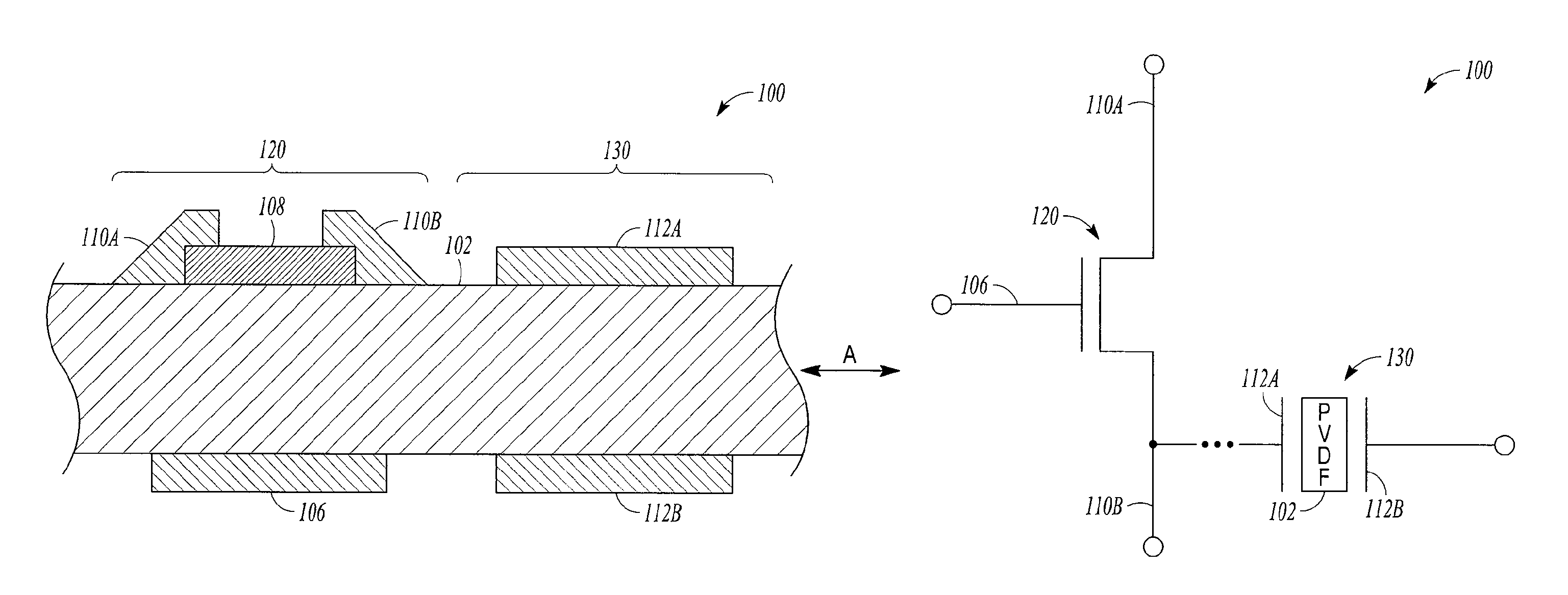
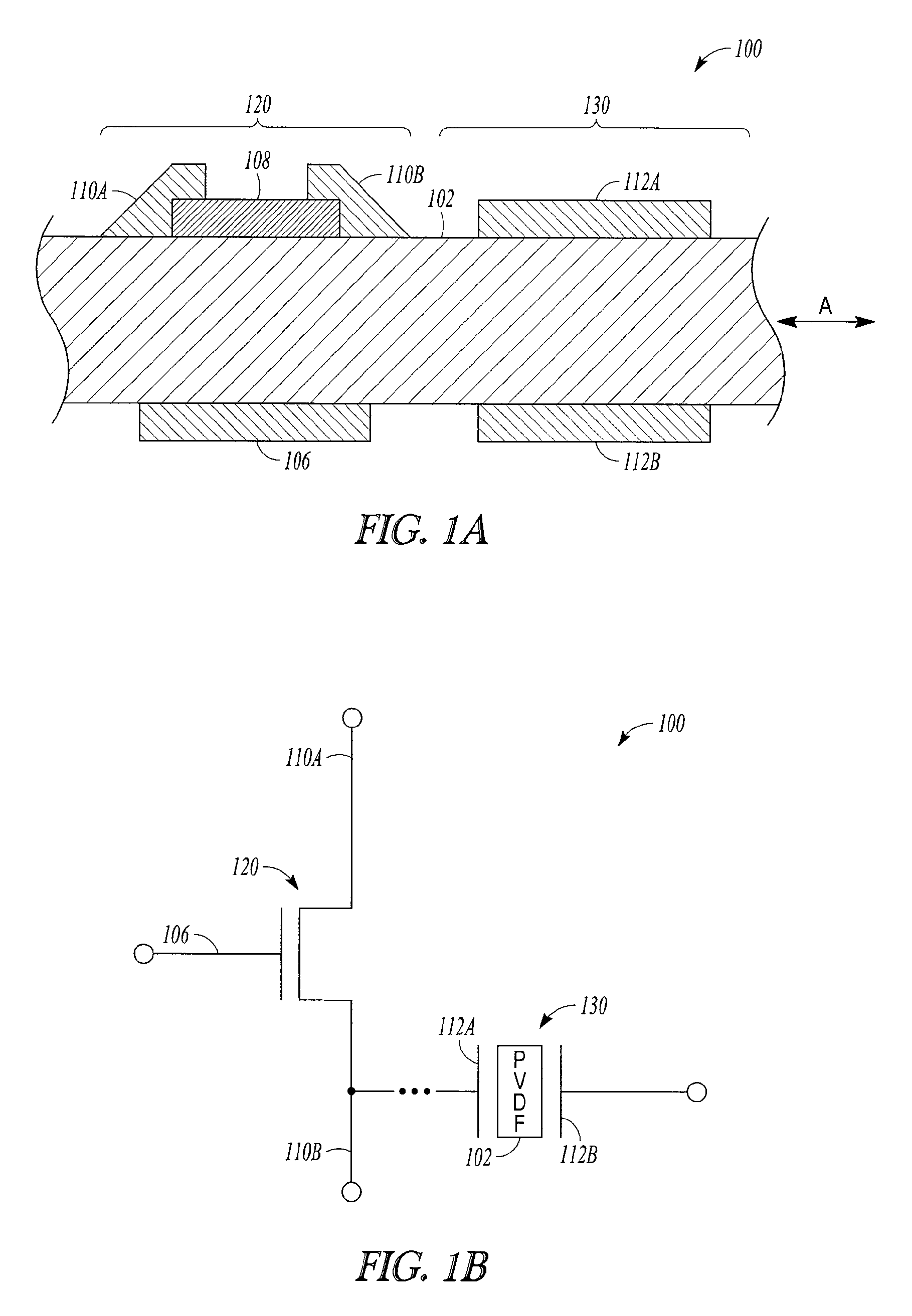
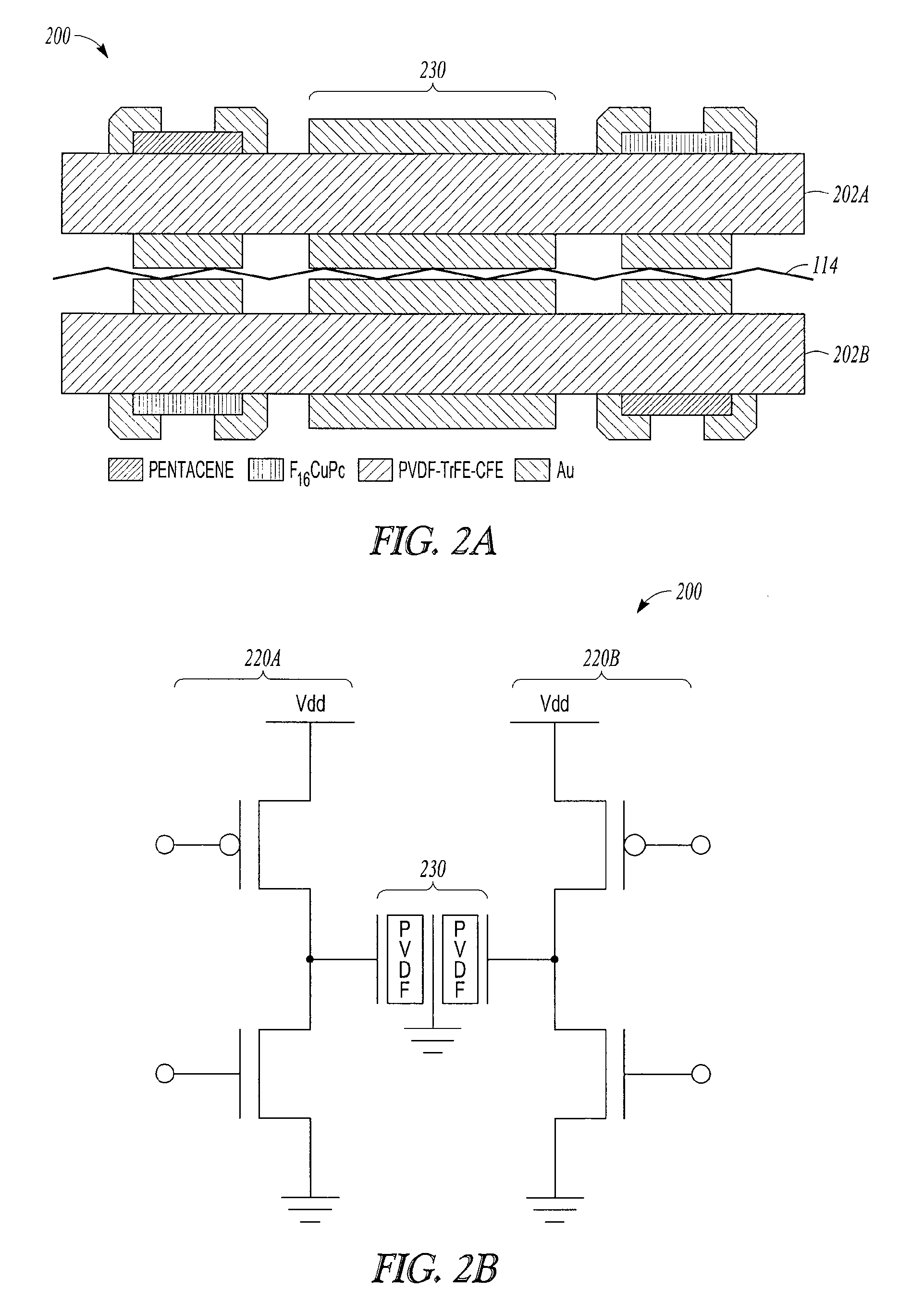
[0051 can include or use subject matter (such as an apparatus, a method, a means for performing acts, or a device readable medium including instructions that, when performed by the device, can cause the device to perform acts), such as can include a first dielectric substrate including a PVDF-TrFe-CFE terpolymer, a first semiconductor region coupled to a first surface of the first dielectric substrate, and a first gate region coupled to a second surface of the first dielectric substrate, the second surface opposite the first surface and opposite the first semiconductor region.

[0052]Example 2 can include, or can optionally be combined with the subject matter of Example 1, to optionally include a first source region and a first drain region respectively electrically coupled to the first semiconductor region, and wherein the first dielectric substrate, the first semiconductor region, the first source region, the first drain region, and the first gate region comprise a first field-effec...


PUM


Abstract

An organic electrical device can include a first dielectric substrate including a PVDF-TrFe-CFE terpolymer, a first semiconductor region coupled to a first surface of the first dielectric substrate, and a first gate region coupled to a second surface of the first dielectric substrate, the second surface opposite the first surface and opposite the first semiconductor region. The organic electrical device can include an organic field-effect transistor (OFET), comprising the first gate region, the first dielectric substrate, a first source region, and a first drain region respectively electrically coupled to the first semiconductor region. An electrostrictive actuator or mechanical sensor can be co-integrated on the first dielectric substrate, the actuator or sensor including first and second conductive regions located on opposite surfaces of the first dielectric substrate. The actuator or sensor can be electrically coupled to the OFET, and controlled at least in part by the OFET.

Description

CLAIM OF PRIORITY[0001]This application is a U.S. National Stage Application filed under 35 U.S.C. §371 of International Application Serial No. PCT / US2012 / 032382, titled “OFET INCLUDING PVDF-TRFE-CFE DIELECTRIC,” filed on 5 Apr. 2012, and published on 18 Jul. 2013 as WO 2013 / 106021, which claims the benefit of priority to U.S. Provisional Patent Application Ser. No. 61 / 472,979, titled “OFET INCLUDING PVDF-TRFE-CFE DIELECTRIC,” filed on Apr. 7, 2011, the benefit of priority of each of which is hereby presently claimed, and each of which is hereby incorporated by reference herein in its respective entirety.BACKGROUND[0002]Field-Effect Transistors (FETs) can include a range of transistor topologies in which charge carriers can flow between a source region and drain region, such as controlled by a voltage applied between a gate region and the source region. FETs can be used in analog or digital applications, such as included as a portion of a monolithic integrated circuit. In one approa...

Claims


Application Information

Patent Timeline
IPC IPC(8): H01L29/08H01L51/40H01L51/00H01L51/05H01L27/28
CPCH01L51/0096H01L51/052H01L27/283H01L51/05Y02E10/549H01L2251/10Y02P70/50H10K19/10H10K77/10H10K10/471H10K10/00H10K71/00
Inventor JIA, ZHANGPERVEZ, NADIACARTA, FABIOKYMISSIS, IOANNIS
Owner THE TRUSTEES OF COLUMBIA UNIV IN THE CITY OF NEW YORK
Why Eureka
Try Eureka