

Method of manufacturing through-glass vias
a technology of glass vias and vias, which is applied in the direction of semiconductor devices, semiconductor/solid-state device details, electrical apparatus, etc., can solve the problems of large device space, high cost, and complicated device contact and packaging, and achieve low cost, high reliability, and low complexity
Inactive Publication Date: 2015-09-08
SCHOTT CORP
View PDF5 Cites 6 Cited by
- Summary
- Abstract
- Description
- Claims
- Application Information
AI Technical Summary
Benefits of technology
This method enables the production of glass substrates with through-glass via holes that are cost-effective, reliable, and suitable for use as interposers, reducing electrical resistance and increasing device density while being compatible with conventional processing technologies.
Problems solved by technology
However, the embodiment of further miniaturization of integrated circuits is costly and the ever more complex circuits require an increasing number of I / O leads, which complicates the contacting and packaging of the devices.
Currently, stacked devices are mostly interconnected by wire bonding, which is a complex process that requires a large amount of space on the device and unnecessarily long connecting leads.
Furthermore, wire bonding commonly gives a fairly high resistance and can be unreliable.
However, it is difficult and expensive to form through-holes through a glass substrate, e.g., it is usual to use laser, sandblasting or ultrasonic wave drill to form through holes.
In such a case, it is difficult and expensive to form micro through-holes, and the application of such a glass substrate is limited now.
The microelectronics industry has had a great deal of trouble forming good via holes inexpensively.
Via holes have been produced, but the complexity and cost structure of generating the through-via hole in a glass substrate are major obstacles.
Method used
View moreImage
Smart ImageViewing Examples

Examples
examples
[0074]Referring to FIG. 5, a glass substrate 50 having a crude mask 51 of paraffin wax was formed on the top surface and orthogonally on the bottom surface of a glass substrate, followed by a glass etch step. An etched channel 52 on the bottom and an etched channel 53 on the top met at a point of intersection (the confluence point), and a through-glass via 54 was formed.
Login to View More PUM
 Abstract
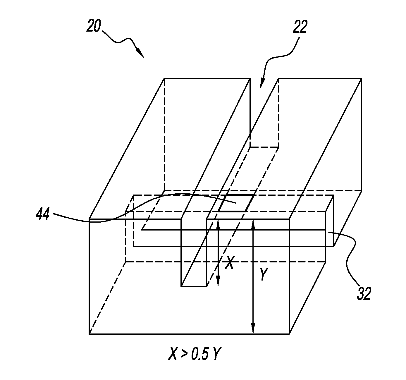
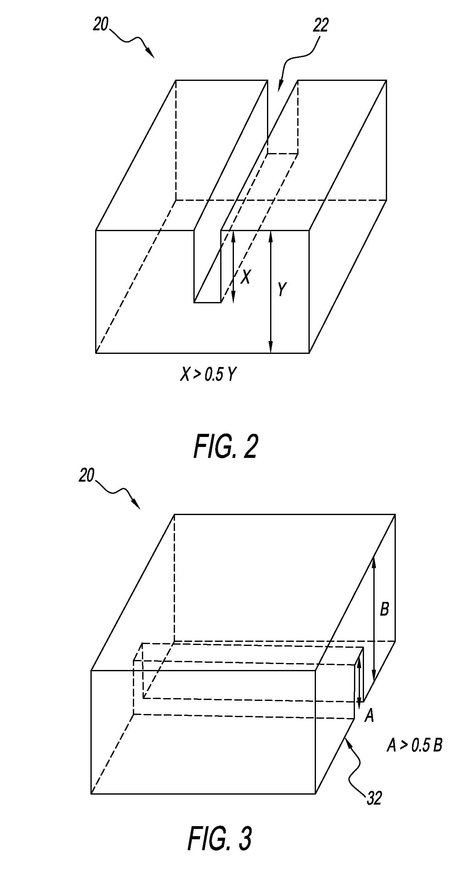
A method of forming a through-glass via hole involves providing a glass substrate having first and second substantially planar parallel surfaces; masking the first and second substantially planar parallel surfaces to form a via-patterned portion thereon; and etching the via-patterned portion on the first and second substantially planar parallel surfaces to form a first channel in the first substantially planar parallel surface and a second channel in the second substantially planar parallel surface. The first channel and second channel are substantially orthogonal or non-orthogonal to one another. The first channel and the second channel intersect to form a quadrilateral through-glass via hole having via openings at the first and second substantially planar parallel surfaces. A low cost, low complexity and high reliability method for producing a glass substrate having a plurality of through-glass via holes such that the glass substrate can be used, for example, as an interposer.
Description
BACKGROUND OF THE DISCLOSURE[0001]1. Field of the Disclosure[0002]This disclosure relates to a method of manufacturing through-glass vias and, in particular, top and bottom channeling of a glass substrate where the top channels and bottom channels are orthogonal or non-orthogonal to each other, and form aligned holes at the point of intersection, with the holes together forming a through-glass via hole.[0003]2. Discussion of the Background Art[0004]In microelectronics, integrated circuit device density is increasing at a high rate. The number of transistors per chip continues to grow. However, the embodiment of further miniaturization of integrated circuits is costly and the ever more complex circuits require an increasing number of I / O leads, which complicates the contacting and packaging of the devices. Hence, other means for getting higher device density are needed. An emerging alternative is to increase the device density per unit area by stacking devices on top of each other. C...
Claims
Login to View More Application Information
Patent Timeline
 Patent Type & AuthorityPatents(United States)
IPC IPC(8): H01L23/48H01L21/768H01L23/498H01L21/48
CPCH01L21/76802H01L21/486H01L23/49827H01L23/49833H01L2924/0002H01L2924/00B81C1/00095
InventorURRUTI, ERIC H.
OwnerSCHOTT CORP