Check patentability & draft patents in minutes with Patsnap Eureka AI!

Robust erase page detection logic for NAND flash memory devices

Active Publication Date: 2015-10-13
CADENCE DESIGN SYST INC
View PDF2 Cites 16 Cited by
  • Summary
  • Abstract
  • Description
  • Claims
  • Application Information

AI Technical Summary

Benefits of technology

The present invention is about a way to make computer systems work better by reducing errors and optimizing activities. It provides a way to determine if a page is available or unavailable for writing to, which can save time and reduce errors. Overall, this invention helps make computer systems faster and more reliable.

Problems solved by technology

Flash memory is popular in applications for consumers because of the robustness of the devices (i.e., shock and water resistance versus disc drives) as well as since flash memory offers fast read access times, as Its mechanical shock resistance helps explain its popularity over hard disks in portable devices; consequently, consumers often expect long-term performance from such devices and are often unfamiliar with the flash endurance limits and disturbance issues that may arise.
It is further understood that within data there may be errors in content resulting from, but not limited to, data bits being flipped (ones are exchanged for zeroes, or vice versa), data being inaccurate, or some data being invalid.
Further, the inherent reliability of flash data may often be affected by a number of factors including: read disturbs, program disturbs, endurance, etc.
BBM is required as bad blocks may result during usage following erase fails, program fails, and read fails.
Similarly, while ECC, in various competencies, is often used to detect and correct the presence of errors to reconstruct the original, error-free data within certain limits, errors may still result even with address correction logic present and often strict error correction approaches may require additional time which thereby further constrains performance.
Contradistinctively, if the cumulative total of data indicates ones totaling less than 4 kB, then the software may conclude that the page is not available for writing as the page has not been erased of prior data or similar even though the page may have been erased, as the discrepancy may have arisen from errors associated with the flash data (i.e., read disturbance, etc.).
This approach, and particularly those that may read a byte at a time, are understood and recognized to be time-intensive processes resulting in overall performance impacts that are not desirable.
This approach often involves reading a byte at a time with reduced performance that are not desirable.
However, since flash devices are inherently erroneous and subject to read disturbances, bits may be flipped more often than is desired such that the approaches in software or in hardware are too time-intensive to implement.
Unfortunately, even after data is written to a flash with error correction (such that when the data of the page is read back that data can be corrected when in error because of the error correction), checking for the correctness or errors associated with the page data requires additional time-intensive processing.
Many of these prior approaches add additional overhead and further limit the utility of the system capacity.

Method used


Image

  • Robust erase page detection logic for NAND flash memory devices
  • Robust erase page detection logic for NAND flash memory devices
  • Robust erase page detection logic for NAND flash memory devices

Examples


Embodiment Construction

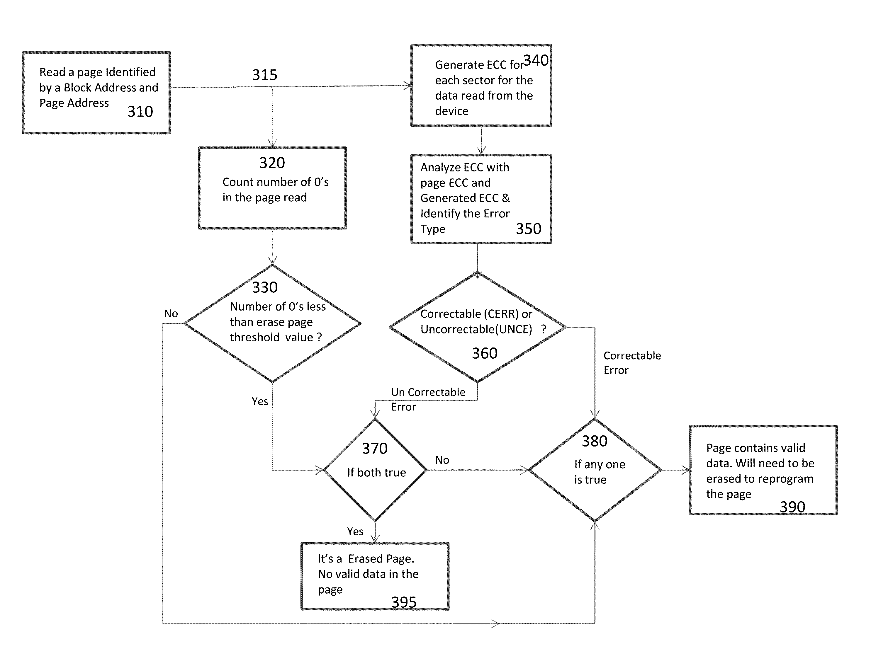
[0025]The following description is presented to enable one of ordinary skill in the art to make and use the invention and is provided in the context of a patent application and its requirements. Various modifications to the preferred embodiments and the generic principles and features described herein will be readily apparent to those skilled in the art. Thus, the present invention is not intended to be limited to the embodiments shown, but is to be accorded the widest scope consistent with the principles and features described herein.

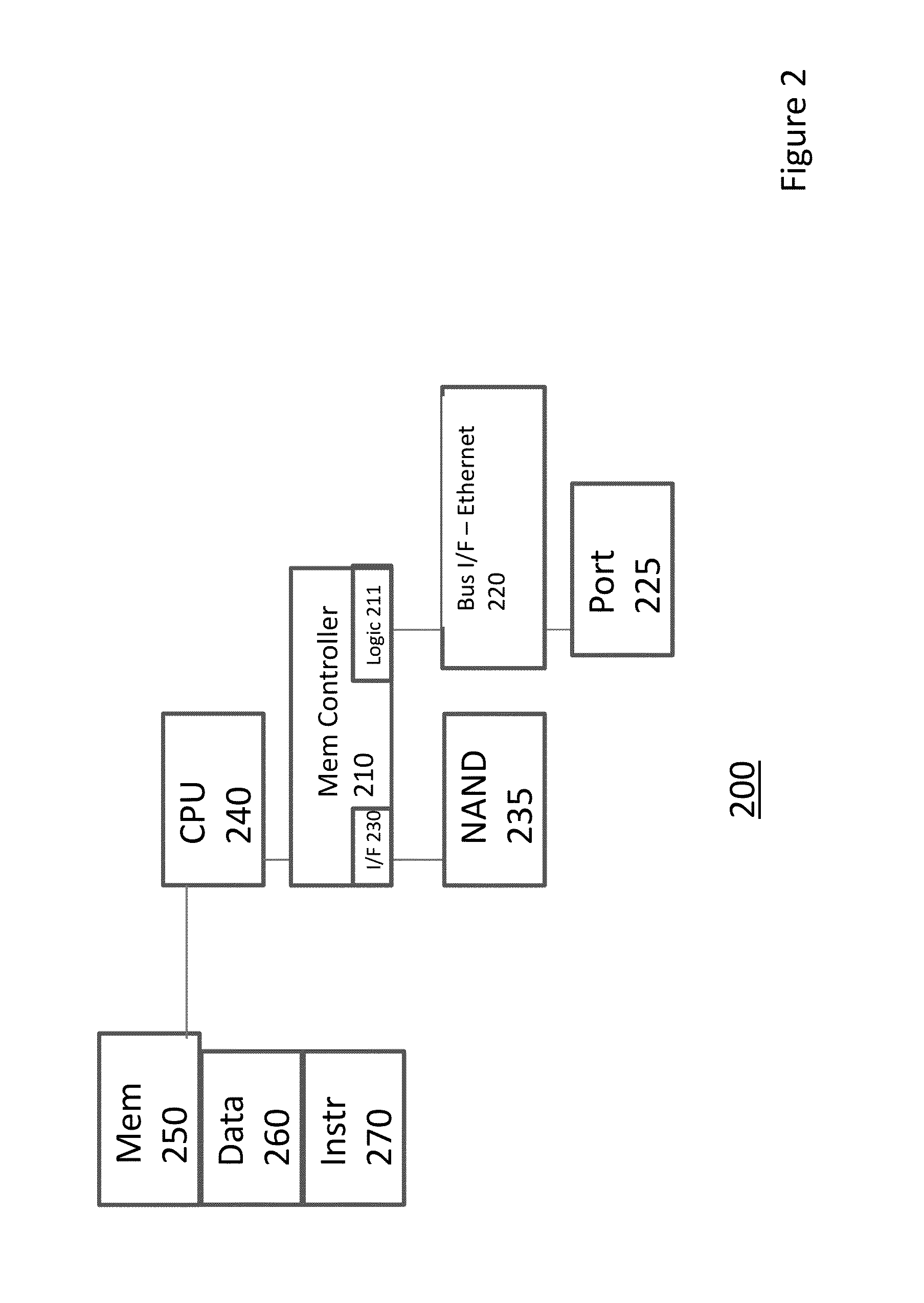
[0026]FIG. 2 sets forth an exemplary block diagram of a NAND flash memory system 200, in accordance with one embodiment of the present invention. From FIG. 2, the system includes a memory controller 210 having logic 211, a bus interface 220 for controlling data exchange to / from external connections 225 and / or busses. The bus interface may include one or more different interfaces. The memory controller may include a NAND flash interface 230 for interfac...


PUM


Abstract

The present invention provides a method and system to reduce the impact of errors introduced in flash devices while providing improved system performance through optimized activities with limited impact to overhead using a predetermined threshold value or threshold device value. In an embodiment, a device threshold value is compared with the cumulative number of data bits having a zero value of a target page and an error type of the target page is assessed to determine whether the target page is available to be written to. Therefore for a highly effective method for is provided for determining the availability of a page, having a block address and page address, to be identified, in one instance, as being an erased page that is available to be written to.

Description

FIELD OF THE INVENTION[0001]The present invention relates generally to Flash memory devices, and more particularly, to effecting improvements by minimizing the effects of error inherency and disturbance events in flash memory devices.BACKGROUND OF THE INVENTION[0002]In typical computer-related devices, there is often a flash memory that involves a NAND-based architecture. The NAND-based architecture typically comprises one or more flash memory chips, a memory controller for executing flash translation code (FTL) code in Read-Only Memory (ROM), a Static Read-Access Memory (SRAM) for maintaining the address mapping information, and a host interface for communicating, such as that of a Personal Computer Memory Card International Association (PCMCIA) for example. In operation, a flash memory device is able to issue commands in association with logical sector addresses of and data resident on the flash device. Within the architecture of the device, commands of read, write, program and / or...

Claims


Application Information

Patent Timeline
IPC IPC(8): G11C16/06G11C16/04
CPCG11C16/0483G11C16/04G11C16/08G11C16/10G06F11/1068
Inventor BRAHMADATHAN, SANDEEPREVANKAR, SRINIVAS SURESH
Owner CADENCE DESIGN SYST INC
Features
  • R&D
  • Intellectual Property
  • Life Sciences
  • Materials
  • Tech Scout
  • Unparalleled Data Quality
  • Higher Quality Content
  • 60% Fewer Hallucinations
Learn More