
FinFET structure with cavities and semiconductor compound portions extending laterally over sidewall spacers

a semiconductor compound and finfet technology, applied in the field of semiconductor compound portions extending laterally over sidewall spacers, can solve problems such as short circuits

Active Publication Date: 2015-10-20
UNITED MICROELECTRONICS CORP
View PDF36 Cites 19 Cited by
  • Summary
  • Abstract
  • Description
  • Claims
  • Application Information

AI Technical Summary

Benefits of technology

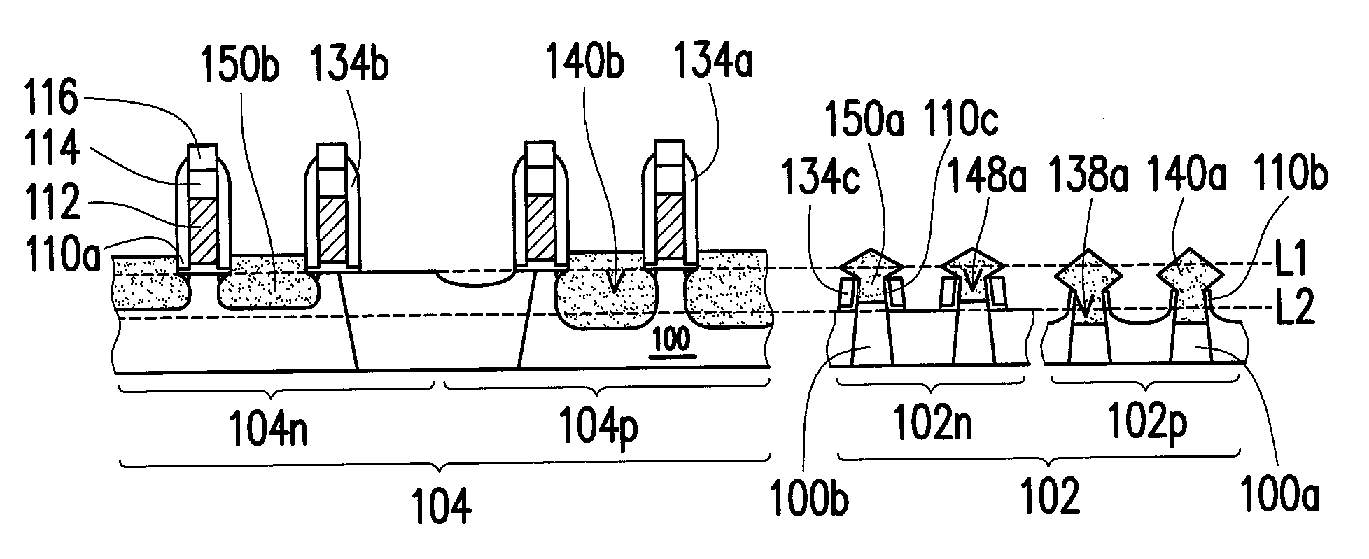
[0012]In the above process of this invention, since the gate dielectric layer is trimmed to reduce the thickness thereof before the spacer material layer is formed, the portions of the spacer material layer on neighboring fins will not merge later, so the spacer material formed over the fins will not be overly thick. In addition, the thinned gate dielectric layer on the top of the fin is easier to remove. As a result, the cavity formed by partial removal of the fin for forming the semiconductor compound is allowed to have a sufficient depth, so that the volume and the strain of the formed semiconductor compound will be sufficient.
[0013]Moreover, since the semiconductor compound is formed from the cavity defined by the surface of the remaining fin and the spacer, the lower portion of the piece of the semiconductor compound is confined by the spacer, so the upper portions of the pieces of the semiconductor compound on neighboring fins will not contact with each other and the process margin can be increased.

Problems solved by technology

However, because the piece of the semiconductor compound grown based on the recessed portions of a fin grows also in the lateral direction, it may contact with a piece of the semiconductor compound on a neighboring fin to cause a short circuit.

Method used


Image

  • FinFET structure with cavities and semiconductor compound portions extending laterally over sidewall spacers
  • FinFET structure with cavities and semiconductor compound portions extending laterally over sidewall spacers
  • FinFET structure with cavities and semiconductor compound portions extending laterally over sidewall spacers

Examples


Embodiment Construction

[0018]It is noted that the following embodiment is intended to further explain this invention but not to limit the scope thereof. For example, though the semiconductor compound of the P-type FinFET is formed first in the embodiment, it is also possible to form the semiconductor compound of the N-type FinFET first in other embodiments. In such cases, it is possible that the first semiconductor compound comprises silicon phosphorous (SiP) and the second semiconductor compound comprises SiGe.

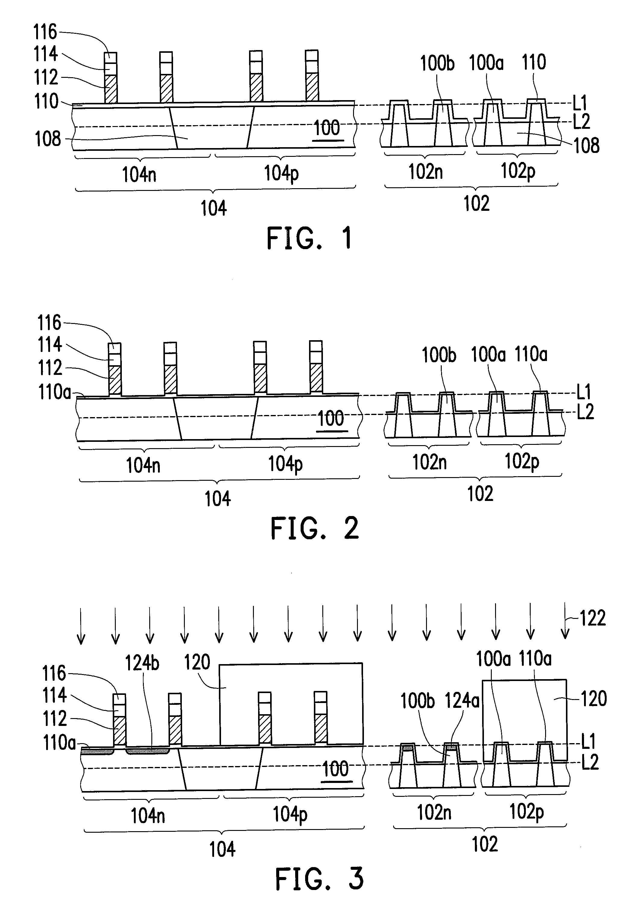
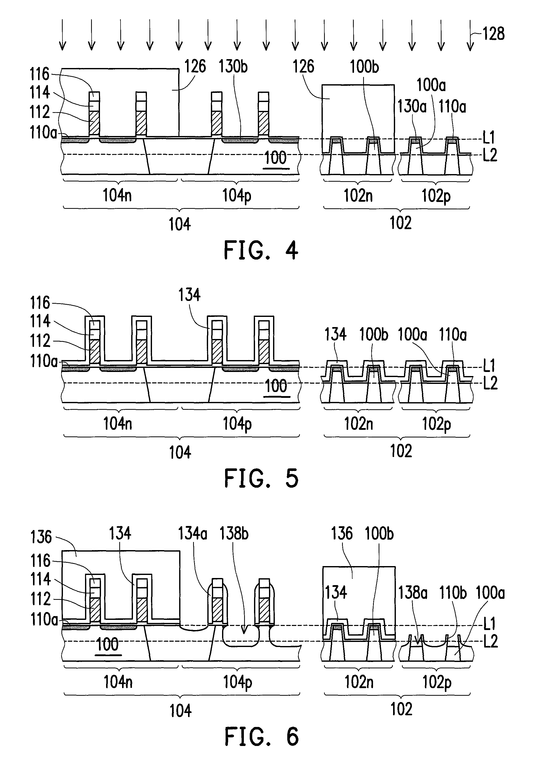
[0019]FIGS. 1-11 illustrate, in a cross-sectional view, a process for fabricating a FinFET structure according to an embodiment of this invention, which is integrated with a fabrication process of ordinary strained CMOS devices.

[0020]Referring to FIG. 1, a semiconductor substrate 100 is provided, which may be a single-crystal silicon substrate. The substrate 100 includes a FinFET area 102 and an ordinary device area 104. The FinFET area 102 includes a NMOS area 102n and a PMOS area 102p. The ordina...


PUM


Abstract

A process for fabricating a fin-type field effect transistor (FinFET) structure is described. A semiconductor substrate is patterned to form a fin. A spacer is formed on the sidewall of the fin. A portion of the fin is removed, such that the spacer and the surface of the remaining fm together define a cavity. A piece of a semiconductor compound is formed from the cavity, wherein the upper portion of the piece of the semiconductor compound laterally extends over the spacer.

Description

BACKGROUND OF THE INVENTION[0001]1. Field of Invention[0002]This invention relates to a semiconductor process and a product thereof, and more particularly relates to a process for fabricating a fin-type field effect transistor (FinFET) structure, and a FinFET structure fabricated through the process.[0003]2. Description of Related Art[0004]A FinFET typically includes a semiconductor fin, a gate crossing over the fin to form a tri-gate structure, and a source and a drain beside the portion of the fin under the gate. In a strained silicon process applied to FinFET, the portions of the fin not under the gate are recessed after the gate is formed, and a semiconductor compound having a lattice parameter different from that of the material of the fin is grown based on the recessed portions of the fin to serve as a source and a drain.[0005]However, because the piece of the semiconductor compound grown based on the recessed portions of a fin grows also in the lateral direction, it may conta...

Claims


Application Information

Patent Timeline
Patent Type & Authority Patents(United States)
IPC IPC(8): H01L29/66H01L29/78H01L21/8238H01L29/165
CPCH01L29/66795H01L21/823807H01L21/823814H01L21/823821H01L29/66636H01L29/785H01L29/7834H01L29/7848H01L29/165
Inventor HUNG, YU-HSIANGFU, SSU-ICHANG, CHUNG-FUWU, YEN-LIANGFAN, CHO-HANLIN, CHIEN-TING
Owner UNITED MICROELECTRONICS CORP
Learn More