Detecting and correcting hard errors in a memory array

a memory array and hard error technology, applied in the field of integrated circuits, can solve problems such as hard errors persisting, soft errors or hard errors, errors occuring,

Active Publication Date: 2015-11-17
ADVANCED MICRO DEVICES INC
View PDF3 Cites 38 Cited by
  • Summary
  • Abstract
  • Description
  • Claims
  • Application Information

AI Technical Summary

Problems solved by technology

Errors occur when values of bits read from one or more of the SRAM cells do not correspond to the values that were intended to be stored in the SRAM cells.
The errors may be characterized as soft errors or hard errors.
Hard errors persist even after the faulty SRAM cell has been re-written.
SRAM arrays are susceptible to hard errors that are produced during manufacturing or arise during the life cycle of the product.
Some of the hard errors produced during manufacturing may be detected during a memory built-in self-test (MBIST) but other manufacturing errors, as well as errors that arise during the lifecycle of the product, may only be manifested at run time.
To illustrate, if an SRAM implemented on a system-on-a-chip (SOC) is operated below its minimum voltage for reliable operation, or if random or environmental conditions affect the state of the SRAM cell, some of the cells in the SRAM may stop functioning correctly and may therefore produce errors even after the faulty SRAM cells have been re-written.
The error may persist for an extended period of time.
Hard errors of this sort can only be detected at runtime because they depend on the particular environmental conditions present when the SRAM array is being read or written.
An error is detected when the stored parity value read out from the array does not match the parity value computed based on the read out data bits from the SRAM cells.
However, hard errors cannot be corrected by re-writing the faulty SRAM cells.
Instead, conventional techniques for detecting and correcting soft errors in SRAM cells may cause the processing device to continuously re-write the faulty SRAM cells without ever correcting the hard error and may even deleteriously affect the functionality of the processing device.
Conventional approaches to error detection and correction in SRAM arrays have a number of drawbacks, particularly when implemented in high-performance computing systems that may need to run continuously for long periods of time without interruption.
Flushing the state of the processing device to physically replace or repair the SRAM in response to detecting a hard error may cause a significant amount of work to be lost, potentially costing the user a significant amount of time and money.
One alternative is to add redundant rows or columns to correct hard errors, but this approach may consume a large amount of area on the processing device.
However, setting aside portions of the SRAM to replace faulty sub-blocks may degrade the performance of the SRAM, e.g., by reducing the amount of memory available in the SRAM.
Furthermore, conventional approaches do not distinguish between activated and deactivated errors.
An activated error is an error that can have a functional, power, or performance impact on the processing device.
If an activated error is not detected, it can cause functional damage to the processes being performed by the processing device.
A de-activated error is an error that may not have a significant functional, power, or performance impact on the processing device.
For example, errors in predictor structures may be classified as de-activated errors because the undetected single bit errors may decrease the accuracy of the prediction but are unlikely to cause a functional impact on the corresponding process.
Conventional replacement techniques assume that all detected errors are permanent activated errors and consequently do not allow for reuse or de-allocation of the resources reserved for replacement of faulty portions of the SRAM.

Method used


Image

  • Detecting and correcting hard errors in a memory array
  • Detecting and correcting hard errors in a memory array
  • Detecting and correcting hard errors in a memory array

Examples


Embodiment Construction

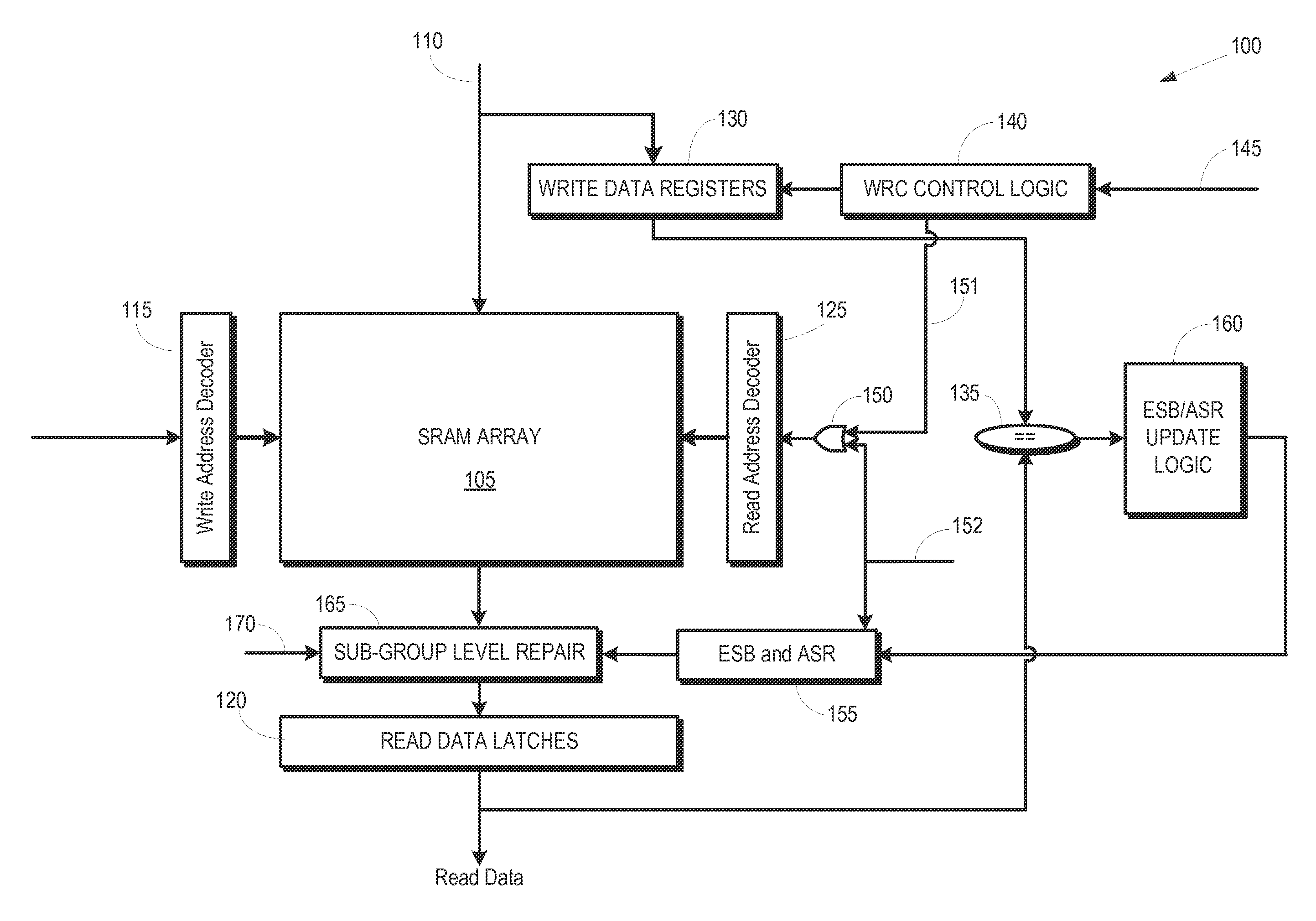
[0022]FIGS. 1-9 describe embodiments of a processing device that can implement run time detection and classification of hard errors in portions of a memory, such as an SRAM array. The hard errors may then be corrected by replacing the faulty portions with reusable entries in an error status buffer. In the event that the hard errors are deactivated or otherwise resolved (e.g., by an increase in the operating voltage of the memory), the reusable entry can be deallocated and subsequently used to correct other hard errors in other portions of the memory. Reusing entries to correct hard errors detected at runtime, which may later resolve, can increase the number of hard errors that may be corrected over the lifetime of the processing device, potentially increasing production yield as well as the operational lifetime of processing devices such as a system-on-a chip (SOC).

[0023]Some embodiments of the processing device initially detect errors using conventional error detection techniques s...


PUM


Abstract

Hard errors in the memory array can be detected and corrected in real-time using reusable entries in an error status buffer. Data may be rewritten to a portion of a memory array and a register in response to a first error in data read from the portion of the memory array. The rewritten data may then be written from the register to an entry of an error status buffer in response to the rewritten data read from the register differing from the rewritten data read from the portion of the memory array.

Description

GOVERNMENT LICENSE RIGHTS[0001]This invention was made with government support under Prime Contract Number DE-AC52-07NA27344, Subcontract Number B600716 awarded by the Department of Energy (DOE). The Government has certain rights in this invention.BACKGROUND[0002]1. Field of the Disclosure[0003]The present disclosure relates generally to integrated circuits and, more particularly, to memory arrays in integrated circuits.[0004]2. Description of the Related Art[0005]In most static random access memory (SRAM) architectures, all of the SRAM cells corresponding to a selected row are written or read out together. Some specific SRAM implementations may selectively write to and read from a subset of the cells in the selected row. Errors occur when values of bits read from one or more of the SRAM cells do not correspond to the values that were intended to be stored in the SRAM cells. For example, an error occurs when a value of “1” is written to an SRAM cell, but a value of “0” is returned w...

Claims


Application Information

Patent Timeline
Patent Type & Authority Patents(United States)
IPC IPC(8): G06F11/10G11C29/52G11C29/42G11C11/41G11C29/04
CPCG06F11/1008G11C29/42G11C29/52G11C11/41G11C2029/0409G11C29/78
Inventor KALAMATIANOS, JOHNJOHN, JOHNSY KANJIRAPALLILGELINAS, ROBERTSRIDHARAN, VILAS K.NEVIUS, PHILLIP E.
Owner ADVANCED MICRO DEVICES INC
Why Eureka
Try Eureka