Vertical nitride semiconductor device and method for manufacturing same

a technology of nitride-based semiconductors and light-emitting devices, which is applied in the direction of semiconductor devices, basic electric elements, electrical apparatus, etc., can solve the problems of small light-emitting area, inability to sufficiently radiate heat generated by the semiconductor layer, and complicated manufacturing methods of nitride-based semiconductor light-emitting devices, etc., to achieve excellent adhesion between the package and the conductive substrate, reduce the temperature of the semiconductor layer, and improve the conductive layer

Inactive Publication Date: 2015-11-24
NICHIA CORP
View PDF15 Cites 0 Cited by
  • Summary
  • Abstract
  • Description
  • Claims
  • Application Information

AI Technical Summary

Benefits of technology

[0010]However, since the entire surface of the conductive substrate and the entire surface of the semiconductor layer are bonded together in the vertical nitride semiconductor device described in JP 2001-007394 A, the area of the bottom surface of the conductive substrate on the side of a package becomes equal to the bonding area of the semiconductor layer when the semiconductor device is mounted and used. As a result, it is not possible to sufficiently radiate heat generated from the semiconductor layer at the bottom surface of the conductive substrate and achieve a high efficiency and a high output.
[0012]The present invention has been made in view of the above problems and has an object of providing a vertical nitride semiconductor device capable of sufficiently radiating heat from a conductive substrate, improving the adhesion between a package and the conductive substrate, and achieving a high efficiency and a high output and a method for manufacturing the same.
[0014]According to the above configuration, the conductive substrate has the flange part, which extends from the side surface of the conductive substrate, on the side of the other front surface thereof such that the area of the other front surface of the conductive substrate becomes larger than that of the bonding front surface of the semiconductor layer. The flange part is formed in a manner in which the conductive substrate and the semiconductor layer are bonded together and then the remaining part of the conductive substrate is divided, the remaining part being formed by cutting off the semiconductor layer and part of the conductive substrate in the thickness direction so as to expose the side surface of the semiconductor layer and the side surface of the conductive substrate. Therefore, the area of the other front surface (bottom surface) of the conductive substrate becomes larger than that of the bonding front surface of the semiconductor layer. As a result, heat radiation is improved at the bottom surface of the conductive substrate on the side of a package and an increase in the temperature of the semiconductor layer is reduced when the semiconductor device is mounted and used. In addition, the adhesion between the package and the conductive substrate is improved.
[0016]According to the above procedure, the flange part extending from the side surface is formed on the side of the other front surface of the conductive substrate by the cutting step and the dividing step. Therefore, the area of the other front surface (bottom surface) of the conductive substrate becomes larger than that of the bonding front surface of the semiconductor layer. As a result, heat radiation is improved at the bottom surface of the conductive substrate on the side of a package and an increase in the temperature of the semiconductor layer is reduced when the semiconductor device is mounted and used. In addition, the adhesion between the package and the conductive substrate is improved.
[0017]Preferably, the dividing step includes forming cut lines in the remaining parts of the conductive substrate from the side of the other front surface of the conductive substrate, thereby dividing the laminating devices. Thus, it is possible to prevent a mounting-side electrode from protruding more than necessary.
[0018]According to a vertical nitride semiconductor device of an embodiment of the present invention, heat is sufficiently radiated from a conductive substrate, and the adhesion between a package and the conductive substrate is excellent. Therefore, it is possible to achieve a high efficiency and a high output. In addition, according to a method for manufacturing the vertical nitride semiconductor device of the embodiment of the present invention, it is possible to provide the vertical nitride semiconductor device that achieves a high efficiency and a high output since heat is sufficiently radiated from the conductive substrate and the adhesion between the package and the conductive substrate is excellent.

Problems solved by technology

As a result, it is not possible to sufficiently radiate heat generated from the semiconductor layer at the bottom surface of the conductive substrate and achieve a high efficiency and a high output.
Therefore, the principal surfaces of the multi-layered metal layer and the multi-layered semiconductor layer become smaller than that of the pattern surface, which results in a small light-emitting area.
Moreover, the method for manufacturing the nitride-based semiconductor light-emitting device is complicated.

Method used


Image

  • Vertical nitride semiconductor device and method for manufacturing same
  • Vertical nitride semiconductor device and method for manufacturing same
  • Vertical nitride semiconductor device and method for manufacturing same

Examples


Embodiment Construction

[0025](Vertical Nitride Semiconductor Device)

[0026]A description will be given, with reference to the drawings, of a vertical nitride semiconductor device according to an embodiment of the present invention.

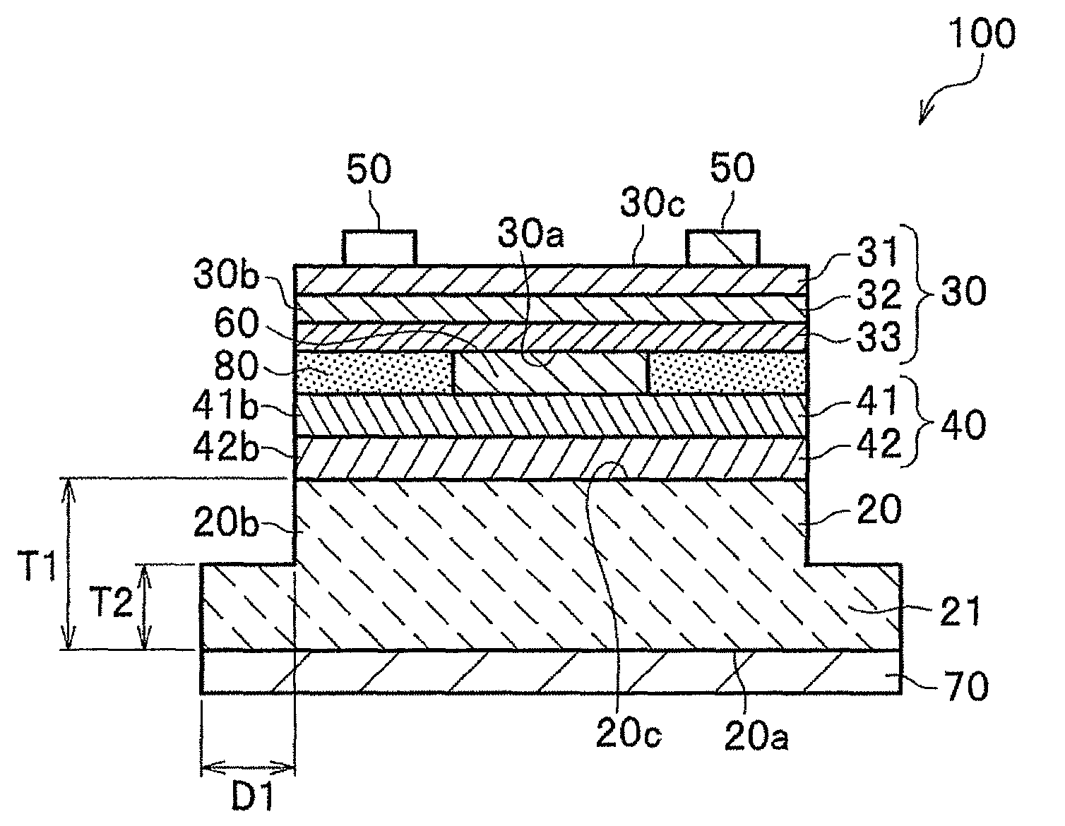
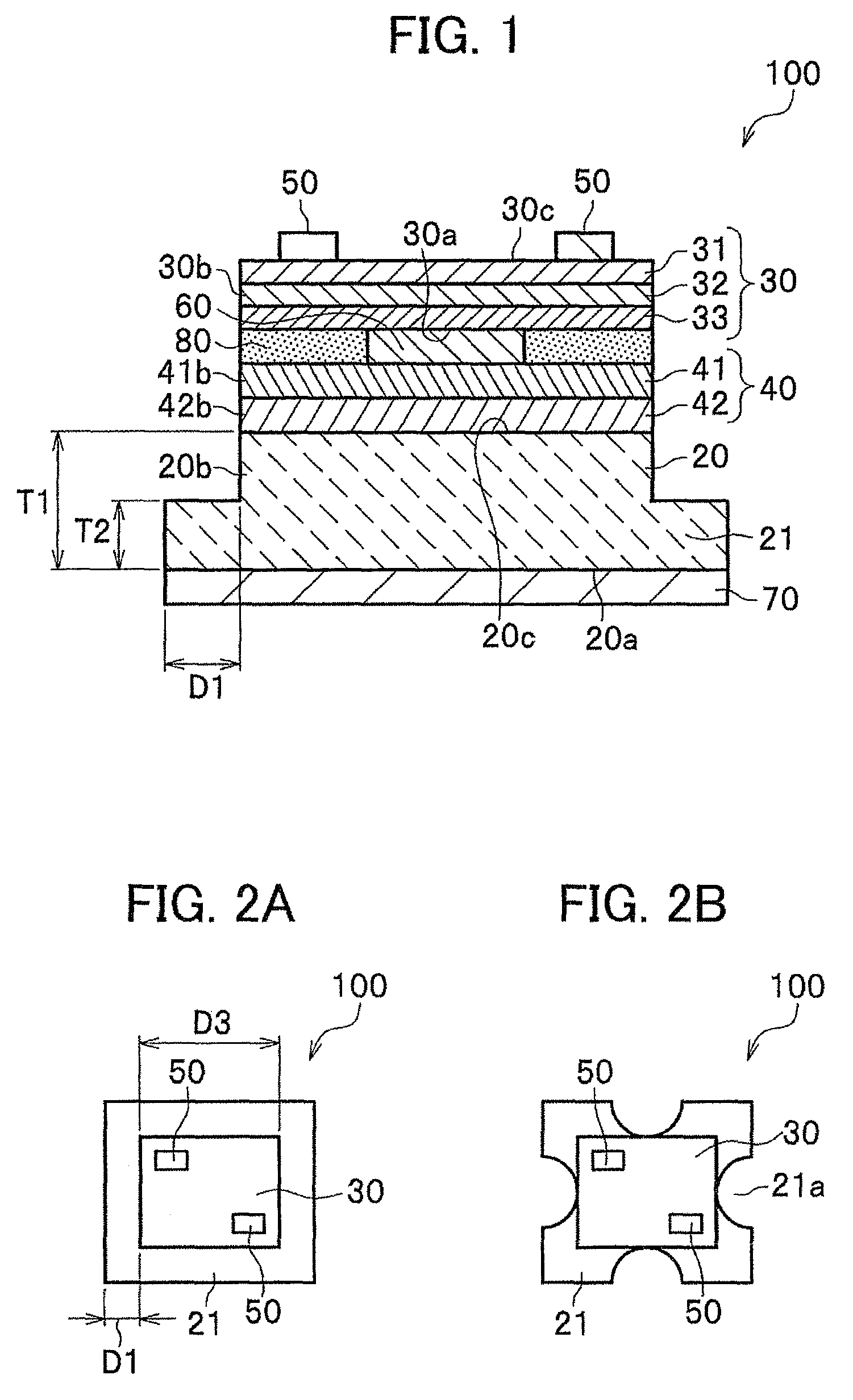
[0027]As shown in FIG. 1, a vertical nitride semiconductor device 100 has a conductive substrate 20, a semiconductive layer 30, a metal layer 70, a first electrode 50, a second electrode 60, and a bonding layer 40. In addition, the conductive substrate 20 has a flange part 21.

[0028]Note that according to the embodiment of the present invention, the vertical nitride semiconductor device 100 refers to one having a semiconductor device structure in which the first electrode 50, the second electrode 60, and the metal layer 70 are arranged in the vertical direction (laminating direction) so as to face each other with the conductive substrate 20 and the semiconductor layer 30 interposed therebetween.

[0029]Next, a description will be given of each configuration of the vertical nitride s...


PUM

PropertyMeasurementUnit
widthaaaaaaaaaa
thicknessaaaaaaaaaa
thickness T1aaaaaaaaaa

Abstract

Disclosed is a vertical nitride semiconductor device including a conductive substrate; a semiconductor layer bonded to the conductive substrate via a second electrode; a metal layer formed on the conductive substrate; a first electrode formed on the semiconductor layer; and a bonding layer formed between the conductive substrate and the second electrode. The conductive substrate has a flange part, which extends from a side surface of the conductive substrate, on a side of the other front surface thereof. The flange part is formed in a manner in which the conductive substrate and the semiconductor layer are bonded together and then a remaining part of the conductive substrate is divided, the remaining part being formed by cutting off the semiconductor layer and part of the conductive substrate in a thickness direction so as to expose a side surface of the semiconductor layer and the side surface of the conductive substrate.

Description

CROSS REFERENCE TO RELATED APPLICATION[0001]The present application claims benefit of the filing date of Japanese Patent Application No. 2012-072442 filed on Mar. 27, 2012, the disclosure of which is incorporated herein by reference.BACKGROUND OF THE INVENTION[0002]1. Field of the Invention[0003]The present invention relates to a nitride semiconductor device for a light-emitting diode (LED), a laser diode (LD), or the like and, in particular, to a high-efficiency high-output vertical nitride semiconductor device and a method for manufacturing the same.[0004]2. Description of the Related Art[0005]Known nitride semiconductor devices for light-emitting diodes or the like include one in which an n-type semiconductor layer, an active layer, and a p-type semiconductor layer each made of nitride are laminated on a sapphire substrate one on another. Since the sapphire substrate is insulative and thus electrodes may not be removed from the side of the substrate, such a semiconductor device i...

Claims


Application Information

Patent Timeline
Patent Type & Authority Patents(United States)
IPC IPC(8): H01L21/00H01L33/00H01L33/32H01L21/76H01L33/20H01L33/64
CPCH01L33/32H01L33/0075H01L33/0079H01L33/0095H01L33/20H01L33/642H01L33/0093H01L33/40H01L33/60H01L33/641
Inventor MATSUDA, YOSHIKAZUOKAMOTO, KAZUTO
Owner NICHIA CORP
Why Eureka
Try Eureka