Semiconductor device

a technology of semiconductor devices and semiconductor components, applied in the direction of semiconductor devices, electrical equipment, transistors, etc., can solve the problems of reducing reliability, particularly the variation and decrease of electrical characteristics of semiconductor devices, and achieve the effect of favorable electrical characteristics and high reliability

Active Publication Date: 2015-12-01
SEMICON ENERGY LAB CO LTD
View PDF133 Cites 8 Cited by
  • Summary
  • Abstract
  • Description
  • Claims
  • Application Information

AI Technical Summary

Benefits of technology

[0013]In view of the above problem, an object of one embodiment of the present invention is to provide a semiconductor device using an oxide semiconductor and having high reliability.
[0014]Miniaturization of a transistor is necessary for high-speed operation, low power consumption, price reduction, high integration, or the like of the transistor.
[0015]Thus, another object of one embodiment of the present invention is to provide a semiconductor device using an oxide semiconductor that is miniaturized and has favorable electrical characteristics.
[0024]One embodiment of the present invention makes it possible to provide a semiconductor device using an oxide semiconductor and having high reliability.
[0025]One embodiment of the present invention makes it possible to provide a semiconductor device using an oxide semiconductor that is miniaturized and has favorable electrical characteristics.

Problems solved by technology

Variation and decrease in electrical characteristics of a semiconductor device are particularly a factor of reduction in the reliability thereof.

Method used


Image

  • Semiconductor device
  • Semiconductor device
  • Semiconductor device

Examples


embodiment 1

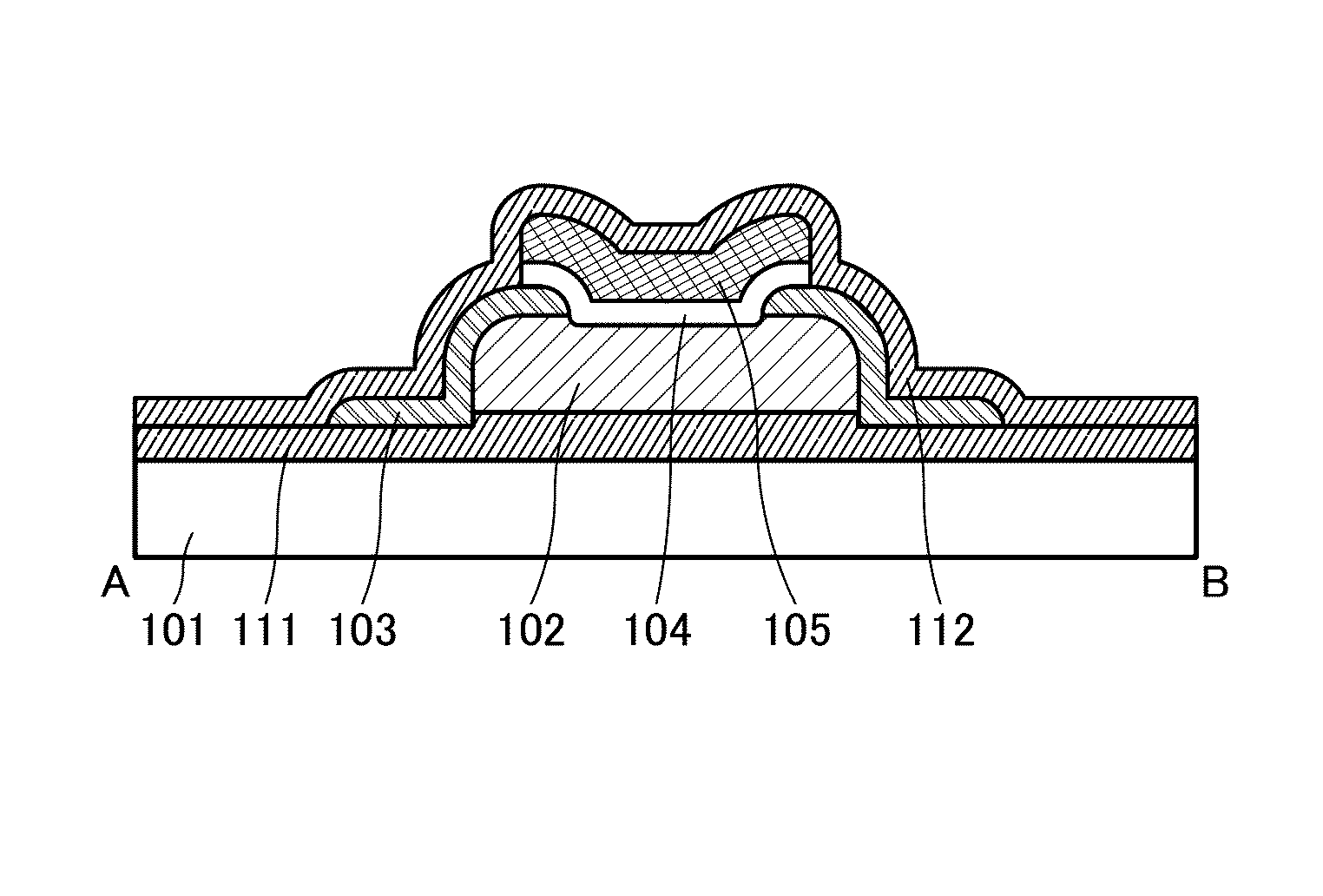
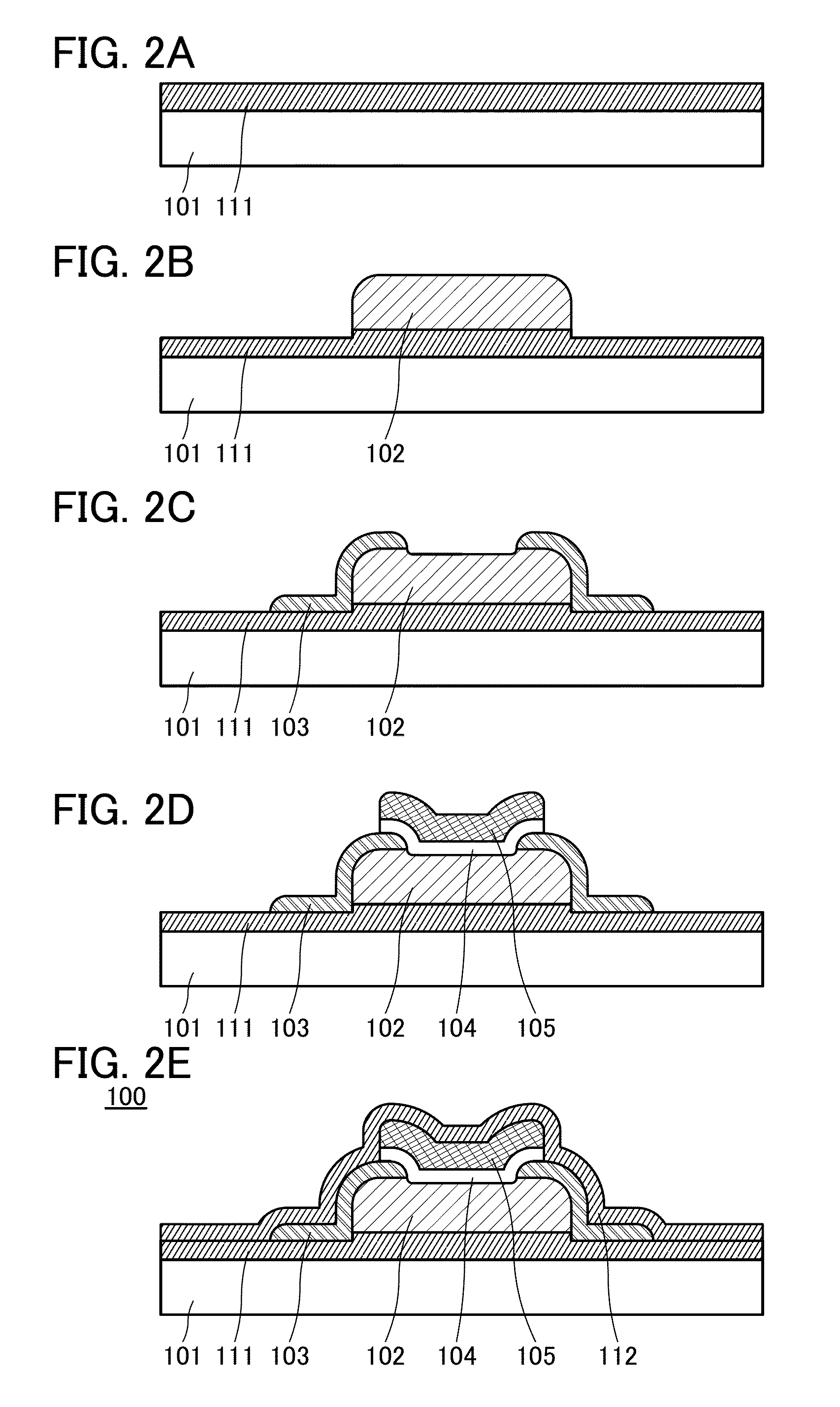
[0060]In this embodiment, a structure and a manufacturing method of a transistor, which is an example of a semiconductor device of one embodiment of the present invention, are described with reference to drawings.

[0061]In the case of manufacturing a transistor using an oxide semiconductor, an oxygen vacancy can be given as a carrier supply source of the oxide semiconductor. A large number of oxygen vacancies in an oxide semiconductor including a channel formation region of a transistor lead to generation of electrons in the channel formation region, which causes defects in electrical characteristics; for example, the transistor becomes normally-on, leakage current increases, or threshold voltage is shifted due to stress application.

[0062]In an oxide semiconductor layer, hydrogen, silicon, nitrogen, carbon, and metal elements which are not the main components are impurities. For example, some hydrogen forms a donor level in the oxide semiconductor layer, which results in an increase ...

example 2

Structural Example 2

[0153]Structural examples of a transistor that are partly different from the structure of the transistor described in the structural example 1 are described below. Note that portions similar to those described above are not described in some cases.

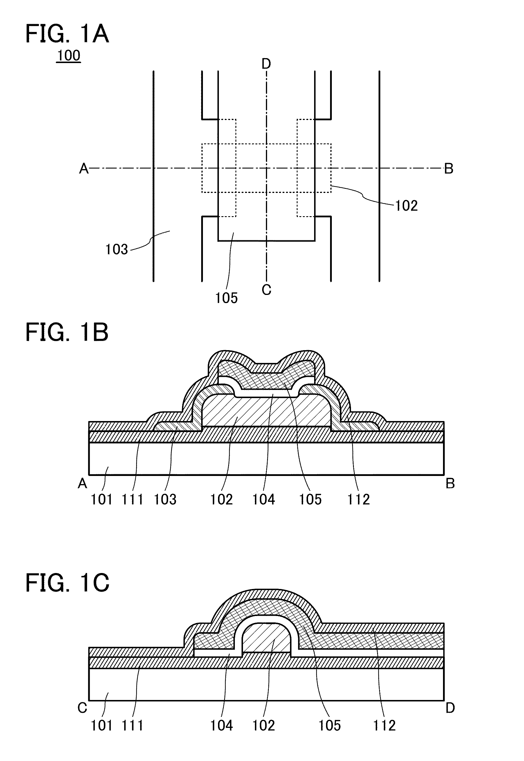
[0154]FIG. 5A is a schematic top view of a transistor 200 described as an example in this structural example. FIG. 5B is a schematic cross-sectional view taken along line E-F in FIG. 5A, and FIG. 5C is a schematic cross-sectional view taken along line G-H in FIG. 5A. Note that some components are not illustrated in FIG. 5A for clarification.

[0155]The transistor 200 includes an insulating layer 207 that is provided over a substrate 201 and includes a groove, a semiconductor layer 202 that is provided over the groove to fill the groove, a pair of electrodes 203 that is provided over the semiconductor layer 202 and electrically connected to the semiconductor layer 202, a gate insulating layer 204 that is over the pair of e...

modification examples

[Modification Examples of Structural Example 2]

[0190]Structural examples of a transistor that are partly different from the structure of the transistor described in the structural example 2 are described below. Note that description of the portions already described is omitted and only different portions are described in detail. Even when positions and shapes of components are different from those in the structural example 2, the same reference numerals are used as long as the components have the same functions as those in the structural example 2, and detailed description thereof is omitted in some cases.


PUM


Abstract

A structure is employed in which a first protective insulating layer; an oxide semiconductor layer over the first protective insulating layer; a source electrode and a drain electrode that are electrically connected to the oxide semiconductor layer; a gate insulating layer that is over the source electrode and the drain electrode and overlaps with the oxide semiconductor layer; a gate electrode that overlaps with the oxide semiconductor layer with the gate insulating layer provided therebetween; and a second protective insulating layer that covers the source electrode, the drain electrode, and the gate electrode are included. Furthermore, the first protective insulating layer and the second protective insulating layer each include an aluminum oxide film that includes an oxygen-excess region, and are in contact with each other in a region where the source electrode, the drain electrode, and the gate electrode are not provided.

Description

BACKGROUND OF THE INVENTION[0001]1. Field of the Invention[0002]The invention disclosed in this specification and the like relates to a semiconductor device and a method for manufacturing the semiconductor device.[0003]In this specification and the like, a semiconductor device means all types of devices that can function by utilizing semiconductor characteristics. A transistor, a semiconductor circuit, an arithmetic unit, a memory device, an imaging device, an electro-optical device, a power generation device (e.g., a thin film solar cell and an organic thin film solar cell), and an electronic device are each an embodiment of the semiconductor device.[0004]2. Description of the Related Art[0005]Attention has been focused on a technique for formation of a transistor using a semiconductor thin film formed over a substrate having an insulating surface. The transistor is applied to a wide range of electronic devices such as an integrated circuit (IC) or an image display device (also sim...

Claims


Application Information

Patent Timeline
Patent Type & Authority Patents(United States)
IPC IPC(8): H01L29/10H01L29/423H01L27/06H01L21/822H01L29/786
CPCH01L29/7869H01L21/8221H01L27/0688H01L29/78696H01L29/78603H01L29/78606H01L29/42384H01L29/4908H01L29/78618
Inventor YAMAZAKI, SHUNPEISUZAWA, HIDEOMIOKAZAKI, YUTAKAMIYAIRI, HIDEKAZU
Owner SEMICON ENERGY LAB CO LTD
Why Eureka
Try Eureka