Solid-state imaging device and imaging system

a solid-state imaging and imaging system technology, applied in the direction of diodes, semiconductor devices, radio-controlled devices, etc., can solve the problems of reduced sensitivity, circuit malfunction, and image signal affecting external noise, so as to reduce the incorporation of external noise

Active Publication Date: 2016-02-02
CANON KK
View PDF29 Cites 11 Cited by
  • Summary
  • Abstract
  • Description
  • Claims
  • Application Information

AI Technical Summary

Benefits of technology

[0007]The present invention is directed to reduce a incorporation of an external noise from a pad into a photoelectric conversion element.
[0009]According to the present invention, it is possible to mitigate incorporation of external noise from the pad into the photoelectric conversion element.

Problems solved by technology

However, the finer the pixels, the smaller the light receiving area of a photoelectric conversion element for detecting light included in the pixels, resulting in a reduction in sensitivity.
In such a construction, external noise from an external terminal is imparted to the circuit of the first substrate, so that a malfunction of the circuit can be generated.
Further, a photoelectric conversion element is arranged on the first substrate, and incorporation of external noise may affect the image signal.

Method used


Image

  • Solid-state imaging device and imaging system
  • Solid-state imaging device and imaging system
  • Solid-state imaging device and imaging system

Examples


Embodiment Construction

[0032]Various exemplary embodiments, features, and aspects of the invention will be described in detail below with reference to the drawings.

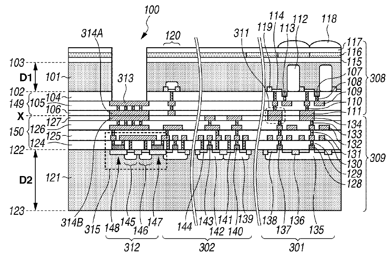
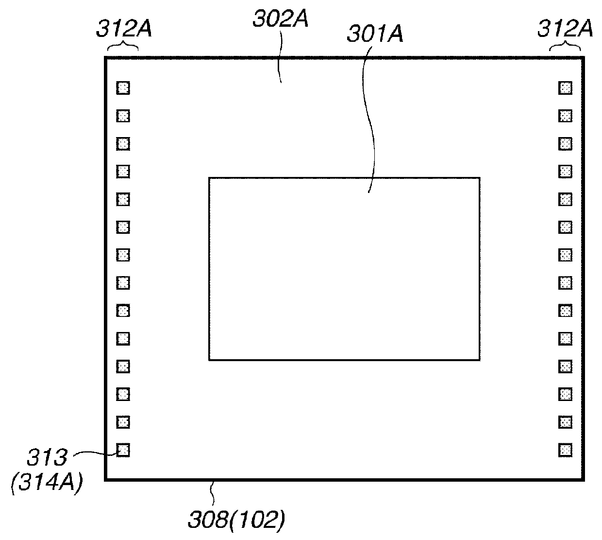
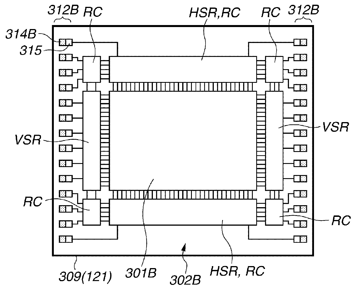
[0033]A solid-state imaging device according to the present invention comprises a first semiconductor substrate including a photoelectric conversion element, and a second semiconductor substrate including at least a part of a peripheral circuit. The peripheral circuit is for generating a signal based on the charge of the photoelectric conversion element and is arranged in a main face thereof. A main face of the first semiconductor substrate and the main face of the second semiconductor substrate are opposed to each other with sandwiching a wiring structure therebetween. The solid-state imaging device comprises a pad to be connected to an external terminal, and a protection circuit electrically connected to the pad and to the peripheral circuit. The protection circuit is arranged in the main face of the second semiconductor substrate. By thus ar...


PUM


Abstract

A solid-state imaging device includes: a first semiconductor substrate including a photoelectric conversion element; and a second semiconductor substrate including at least a part of a peripheral circuit arranged in a main face of the second semiconductor substrate, the peripheral circuit generating a signal based on the charge of the photoelectric conversion element, a main face of the first semiconductor substrate and the main face of the second semiconductor substrate being opposed to each other with sandwiching a wiring structure therebetween; a pad to be connected to an external terminal; and a protection circuit electrically connected to the pad and to the peripheral circuit, wherein the protection circuit is arranged in the main face of the second semiconductor substrate.

Description

TECHNICAL FIELD[0001]The present invention relates to a solid-state imaging device and, in particular, to a pad part thereof.BACKGROUND ART[0002]In a charge-coupled device (CCD) type or an amplification type solid-state imaging device used in a digital still camera, a cam coder or the like, there is a demand for finer pixels to obtain a high definition image. However, the finer the pixels, the smaller the light receiving area of a photoelectric conversion element for detecting light included in the pixels, resulting in a reduction in sensitivity.[0003]Japanese Patent Application Laid-Open No. 2006-191081 discusses complementary metal-oxide-semiconductor (CMOS) type, which is also an amplification type, solid-state imaging device of a construction in which a first substrate with a photoelectric conversion element and a transfer transistor arranged thereon and a second substrate with another circuit arranged thereon are bonded to each other to form a solid-state imaging device to secu...

Claims


Application Information

Patent Timeline
Patent Type & Authority Patents(United States)
IPC IPC(8): H01L27/146H01L27/28H01L27/02
CPCH01L27/146H01L27/0255H01L27/0296H01L27/1464H01L27/14636H01L27/14685H01L27/288H01L27/14645H01L27/14689H04N25/79H10K65/00
Inventor KOBAYASHI, MASAHIROSHIMOTSUSA, MINEO
Owner CANON KK
Why Eureka
Try Eureka