Nanowire transistor structures with merged source/drain regions using auxiliary pillars

Inactive Publication Date: 2016-02-09
IBM CORP
View PDF32 Cites 32 Cited by
  • Summary
  • Abstract
  • Description
  • Claims
  • Application Information

AI Technical Summary

Benefits of technology

[0003]Principles of the present disclosure provide an exemplary fabrication method that includes obtaining a first structure including a base substrate, a plurality of gate structures on the base substrate, and a plurality of semiconductor fin structures on the base substrate, each of the gate structures including a gate conductor and one or more nanowires extending through the gate conductor

Problems solved by technology

For sub-10 nm gate lengths, replacement gate (RMG) processes can be challenging due to the small available volume and gate resistance constraints.
The handling of nanowires in the source/drain regions after spacer reactive ion etch (RIE) and cleaning the space

Method used


Image

  • Nanowire transistor structures with merged source/drain regions using auxiliary pillars
  • Nanowire transistor structures with merged source/drain regions using auxiliary pillars
  • Nanowire transistor structures with merged source/drain regions using auxiliary pillars

Examples


Embodiment Construction

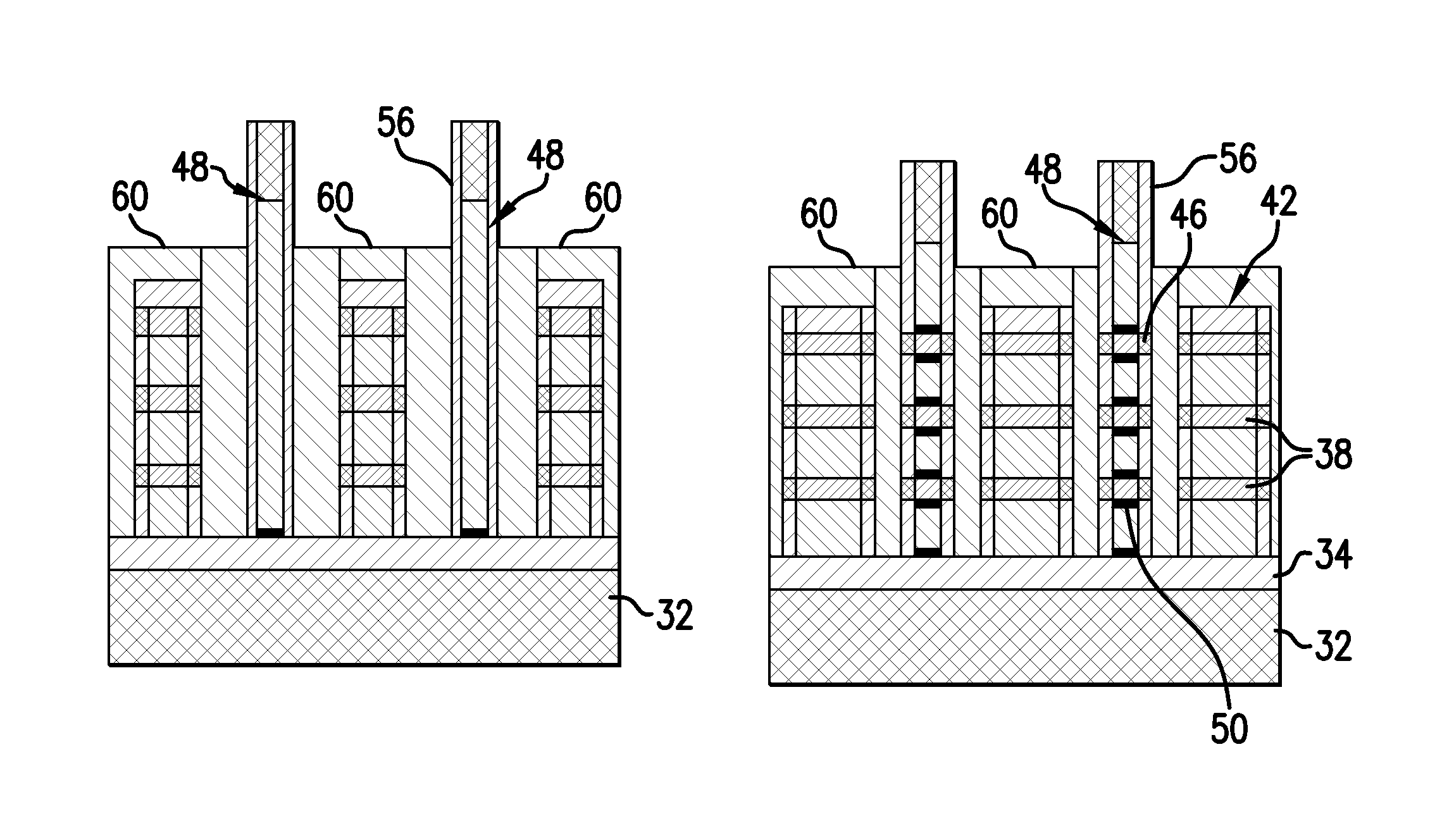
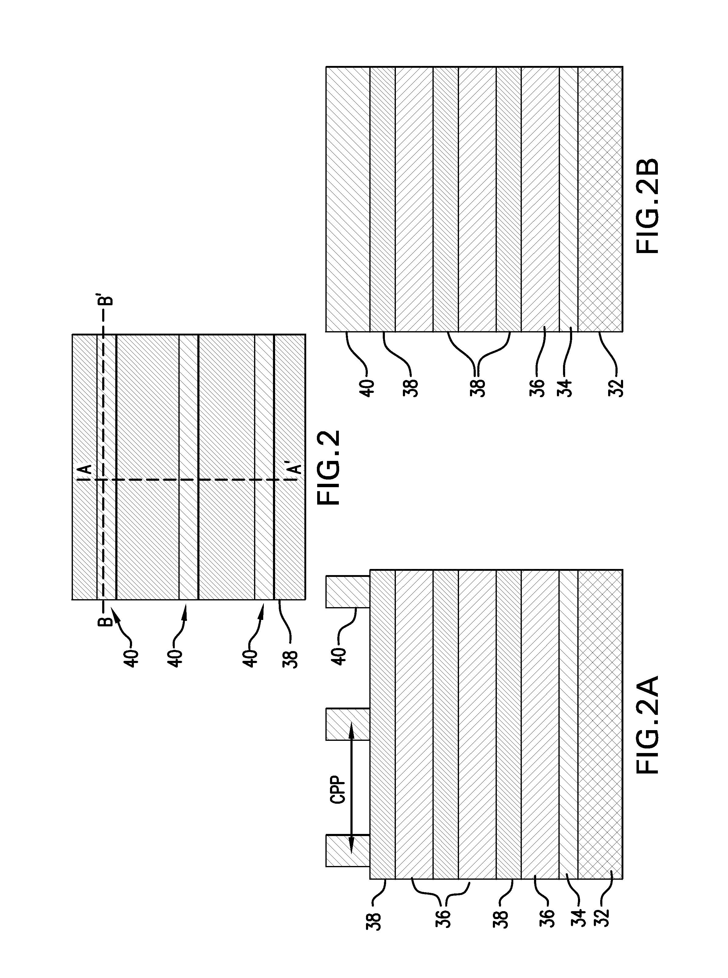
[0020]Fabrication of a gate-all-around nanowire transistor is facilitated by using auxiliary epitaxial nucleation source / drain fin structures formed as pillars on a substrate. The pillars are formed at the same level as the active region (RX) and have a pitch similar to the gate pitch (CPP) of the transistor to be fabricated.

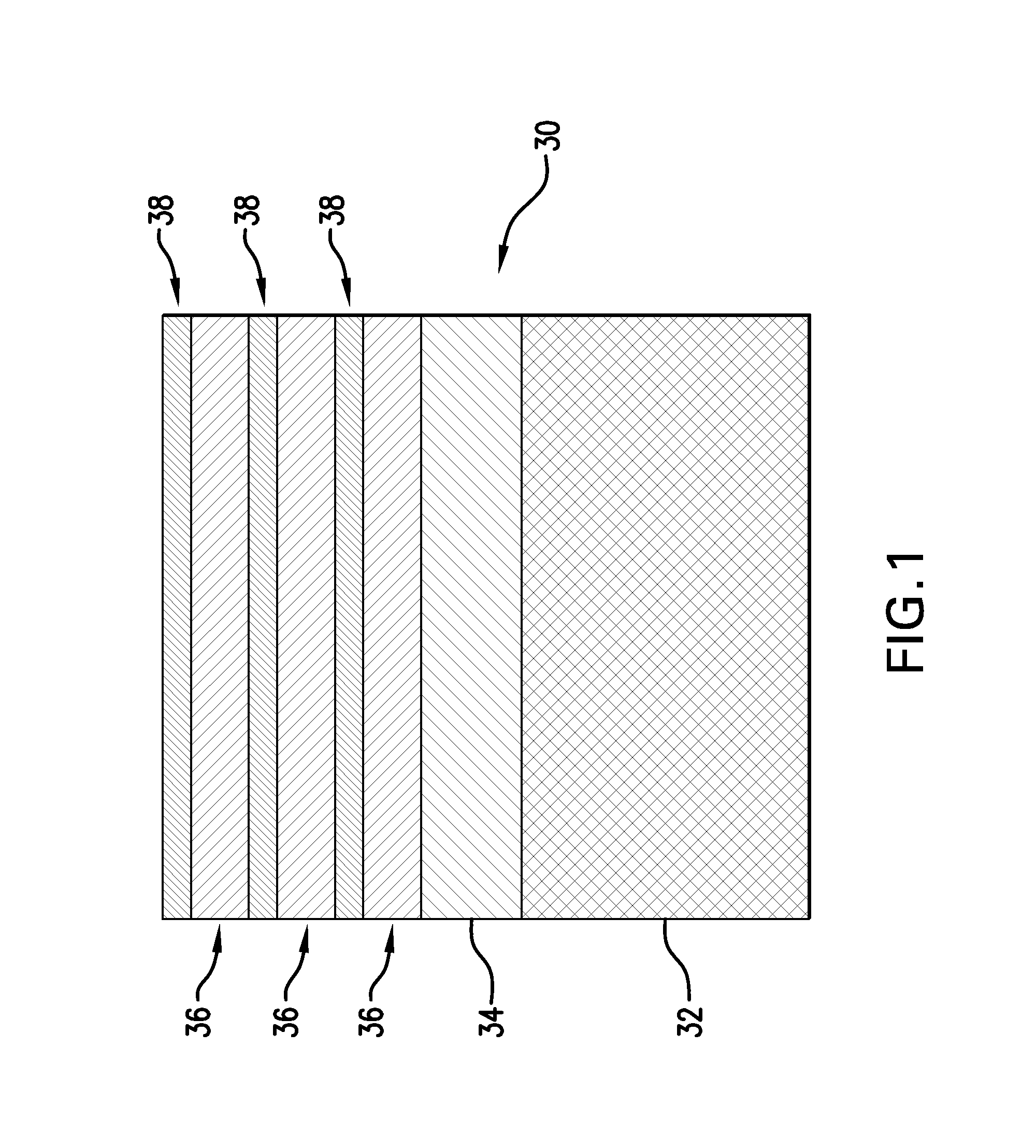
[0021]FIG. 1 illustrates a structure 30 that is employed in one or more embodiments as a starting substrate. The base layer 32 can be bulk silicon, silicon germanium, or germanium on silicon in some embodiments. Other semiconductor materials such as III-V compound semiconductor materials may be employed in some embodiments. Multilayers of the semiconductor materials can also be used to form the base layer 32. In some embodiments, the base layer is a non-semiconductor material including, for example, a dielectric material and / or a conductive material. An electrically insulating layer 34, such as silicon dioxide or a high-k oxide such as hafnium oxide, aluminum ox...


PUM


Abstract

A nanowire transistor structure is fabricated by using auxiliary epitaxial nucleation source/drain fin structures. The fin structures include semiconductor layers integral with nanowires that extend between the fin structures. Gate structures are formed between the fin structures such that the nanowires extend through the gate conductors. Following spacer formation and nanowire chop, source/drain regions are grown epitaxially between the gate structures.

Description

FIELD[0001]The present disclosure relates to the physical sciences, and, more particularly, to field effect transistor (FET) structures and methods of fabrication thereof.BACKGROUND[0002]Gate-all-around (GAA) nanowire field effect transistors having small nanowire diameters are among the CMOS transistor architectures having advantageous device characteristics. For sub-10 nm gate lengths, replacement gate (RMG) processes can be challenging due to the small available volume and gate resistance constraints. The handling of nanowires in the source / drain regions after spacer reactive ion etch (RIE) and cleaning the spacer under the wires in a stacked nanowire architecture is difficult. Methods have been proposed to chop the nanowires and regrow epitaxially from the nanowire corners. For sub-4 nm nanowire dimensions, source / drain epitaxial growth and merging the nanowires is difficult, particularly for pFET devices, due to the small available surface areas and facet issues.SUMMARY[0003]Pr...

Claims


Application Information

Patent Timeline
IPC IPC(8): H01L29/775H01L29/786H01L21/02H01L29/423H01L29/66H01L29/06
CPCH01L29/66439H01L21/02507H01L29/0673H01L29/42392H01L29/775H01L29/78696B82Y10/00H01L29/068H01L29/0669H01L29/41791H01L29/6656H01L29/66795H01L29/785H01L2029/7858H01L21/823807H01L21/823814H01L21/823828H01L27/092H01L29/78618
Inventor HASHEMI, POUYAKHAKIFIROOZ, ALIREZNICEK, ALEXANDER
Owner IBM CORP
Why Eureka
Try Eureka