Organic electronic devices prepared using decomposable polymer additives

a technology of organic electronic devices and additives, applied in the field of organic electronic devices prepared using decomposable polymer additives, can solve problems such as achieve the effects of improving processability of solar cell devices, lowering overall device efficiency/performance, and increasing solution viscosity

Inactive Publication Date: 2016-02-16
RGT UNIV OF CALIFORNIA +1
View PDF13 Cites 4 Cited by
  • Summary
  • Abstract
  • Description
  • Claims
  • Application Information

AI Technical Summary

Benefits of technology

[0006]One advantage of using decomposable binders / polymers instead of washable polymer additives with organic semiconductors in OLED and other electronic devices is that the majority of conventional organic semiconductors are soluble in the solvents used to wash away the polymer additives. Thus in attempting to wash away most of the washable polymer additives from the device layer, some of the organic semiconductor will also be removed, thereby lowering overall device efficiency / performance. Accordingly, in one embodiment, the polymer additives are removed from the device layer without employing any washing steps to remove the polymer additives.
[0007]We incorporated a degradable poly(propylene carbonate) (PC) polymer additive into the BP precursor solution and showed increase solution viscosity and improve processability of solar cell devices. This allows for greater flexibility in film preparation techniques such as slot coating, blade coating, inkjet printing, dip coating, and screen printing, which are processes more suited to large area fabrication. For instance, such areas considered ‘large’ can include, but are not limited to areas of 0.1 square meters or larger. The disclosed PC polymer additive used in the preparation of benzoporphyrin / fullerene solar cells does not diminish efficiency. The PC fully decomposes on annealing and does not change the crystal structure or texturing of BP. Furthermore, the addition of the PC causes a more nanostructured morphology to form in the BP, allowing a bulk heterojunction to form between the BP and the PCBNB which is added afterwards. Devices with this bulk heterojunction exhibit comparable performance to the previously used method of mixing the BP and PCBNB to create a bulk heterojunction. Another advantage of using the former method is that the size of the BP crystallites and gaps is not determined by the acceptor, making the method more extendable to different acceptors.

Problems solved by technology

Thus in attempting to wash away most of the washable polymer additives from the device layer, some of the organic semiconductor will also be removed, thereby lowering overall device efficiency / performance.

Method used


Image

  • Organic electronic devices prepared using decomposable polymer additives
  • Organic electronic devices prepared using decomposable polymer additives
  • Organic electronic devices prepared using decomposable polymer additives

Examples


example 1

Fabrication of Device A

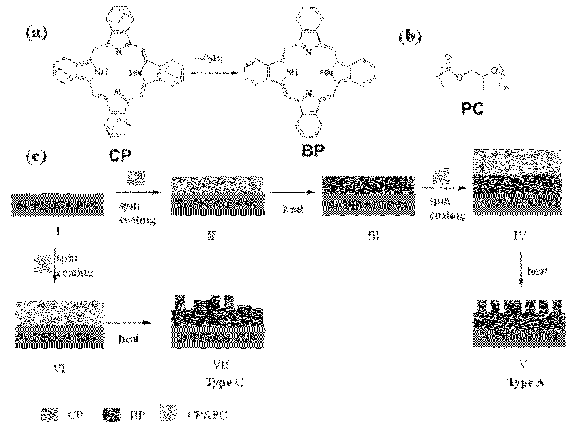
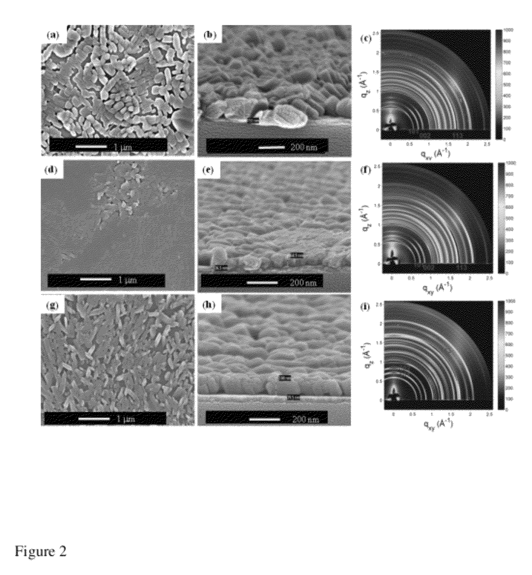
[0077]We fabricated device A using the compound in FIG. 3 according to the following procedure. The ITO layer on a glass substrate was 145 nm thick with a sheet resistance of 8 ohms / square. The 5 mm wide stripe pattern on the ITO layer was etched by conventional photolithographic techniques. Prior to the formation of the buffer layer, the patterned ITO glass was ultrasonically cleaned using surfactant, rinsed in deionized water and finished with an air plasma treatment. The PEDOT:PSS (Clevios AI4083) layer was formed on the ITO substrate by spin coating (3,000 rpm) from an aqueous dispersion to give a smooth, 30 nm thick film. The coated PEDOT:PSS layer was baked for 10 minutes at 120° C. in air and annealed for 3 minutes at 195° C. in a nitrogen glove box just prior to use. The solution of 1.0 wt % CP and PC (3:1 weight ratio) in a mixture of chloroform:chlorobenzene (1:1 weight ratio) was spin-cast (1500 rpm) on the PEDOT:PSS layer in a nitrogen glove box. T...

example 2

Fabrication of Device B

[0078]Device B was fabricated in a same way as device A except the process of coating BP layer. BP layer was formed on the PEDOT:PSS layer by spin coating (1500 rpm) from 0.5 wt % CP solution in a mixture of chloroform:chlorobenzene (1:2 weight ratio). Thermal conversion of the CP to BP was then carried out at 195° C. for 20 minutes in a nitrogen glove box. The solution of 1.0 wt % CP and PC (3:1 weight ratio) in a mixture of chloroform:chlorobenzene (1:1 weight ratio) was subsequently spin-cast (1500 rpm) on the thus coated layer in a nitrogen glove box. After that, the device B was fabricated in the same way as device A. The OPV characteristics of device B was summarized in Table 2.

example 3

Fabrication of Device C

[0079]Device C was fabricated in a same way as device B except the solution of CP and PC mixture. The solution for device C was 1.0 wt % CP and PC (3:1 weight ratio) in a mixture of chloroform: 2-chloroethanol (2.5:1 weight ratio). The OPV characteristics of device C was summarized in Table 2.


PUM

PropertyMeasurementUnit
decomposition temperatureaaaaaaaaaa
areasaaaaaaaaaa
temperatureaaaaaaaaaa

Abstract

A method of fabricating an organic device is provided comprising providing a first solution comprising an organic semiconductor or a precursor thereof; a solvent and a decomposable polymer additive, where the polymer additive is heated so that it decomposes into gas. The method is applicable to large scale fabrication of OLEDs, OPVs and OFET devices.

Description

CROSS REFERENCE TO RELATED APPLICATIONS[0001]This application claims the benefit of Provisional Patent Application No. 61 / 429,653, filed on Jan. 4, 2011, which is incorporated by reference herein in its entirety.FIELD OF THE INVENTION[0002]The invention relates generally to an apparatus and method for producing electronic devices. More particularly, it relates to the use of decomposable polymer additives for producing organic electronic devices.BACKGROUND OF THE INVENTION[0003]Organic photovoltaics (OPV)[1-7] based on single active layer bulk heterojunction comprising a pair of materials where electron transfer occurs from a donor material to an acceptor material where the pair forms a layer with a higher surface area than a simple flat bilayer structure have been drawing attention because they can be processed from solution at low cost and energy consumption. The most conventional OPV devices consisting of an electron donating polymer such as P3HT and an electron accepting material...

Claims


Application Information

Patent Timeline
Patent Type & Authority Patents(United States)
IPC IPC(8): H01L51/46B82Y30/00C07D487/22B82Y40/00H01L51/00B82Y10/00H01L51/05H01L51/42
CPCC07D487/22B82Y10/00B82Y30/00B82Y40/00H01L51/0007H01L51/0026H01L51/004H01L51/0037H01L51/0046H01L51/0077H01L51/0558H01L51/4253Y02E10/549H10K71/15H10K71/40H10K85/141H10K85/211H10K85/1135H10K85/30H10K10/484H10K30/30
Inventor HAWKER, CRAIG J.CHABINYC, MICHAELKU, SUNG-YULIMAN, CHRISTOPHERARAMAKI, SHINJIWANG, HENGBINNIINOMI, TAKAAKI
Owner RGT UNIV OF CALIFORNIA
Why Eureka
Try Eureka