Electro-optic grating modulator

a technology of optoelectronic modulators and grating beams, which is applied in the field of optoelectronic modulators, can solve the problems of limiting the frequency response of the modulator, increasing the group delay of the light, and the modulator has not been achieved in the past, and achieves moderately large signal bandwidth, large change in light intensity, and strong modulation depth

Active Publication Date: 2016-05-10
HRL LAB
View PDF70 Cites 15 Cited by
  • Summary
  • Abstract
  • Description
  • Claims
  • Application Information

AI Technical Summary

Benefits of technology

[0015]Compared to a grating that does not have a velocity matched electrode, this invention achieves stronger modulation depth (larger change in the intensity of light for the same modulation-controlling electric-field strength) while also being capable of high-frequency modulation with moderately large signal bandwidth. Compared to a phase-to-intensity modulator such as a Mach-Zehnder interferometer that has a traveling-wave electrode, this invention achieves the same modulation depth with a physically shorter device. Compared to an electro-absorption modulator that has a traveling-wave electrode, this invention can make use of a dielectric electro-optic material instead of a semiconductor material. Thus, the modulator of this invention can have a much higher electrical breakdown field strength compared to an electro-absorption modulator. This high breakdown field strength makes this modulator more robust when the modulator is exposed to high-energy EM fields whose intensity may be much higher than the intensity of the RF signal.

Problems solved by technology

Thus, the capacitance of that electrode limits the frequency response of the modulator.
However, these increases in the grating length and index step also increase the group delay of the light.
Although there has been a long-standing desire to improve the modulation frequency achieved with optical grating intensity modulators, such a modulator has not been achieved in the past.
Any direct intensity modulation of the light directly by the gratings of these prior art modulators is undesirable and would interfere with the desired operation of the Mach Zehnder modulators.

Method used


Image

  • Electro-optic grating modulator
  • Electro-optic grating modulator
  • Electro-optic grating modulator

Examples


Embodiment Construction

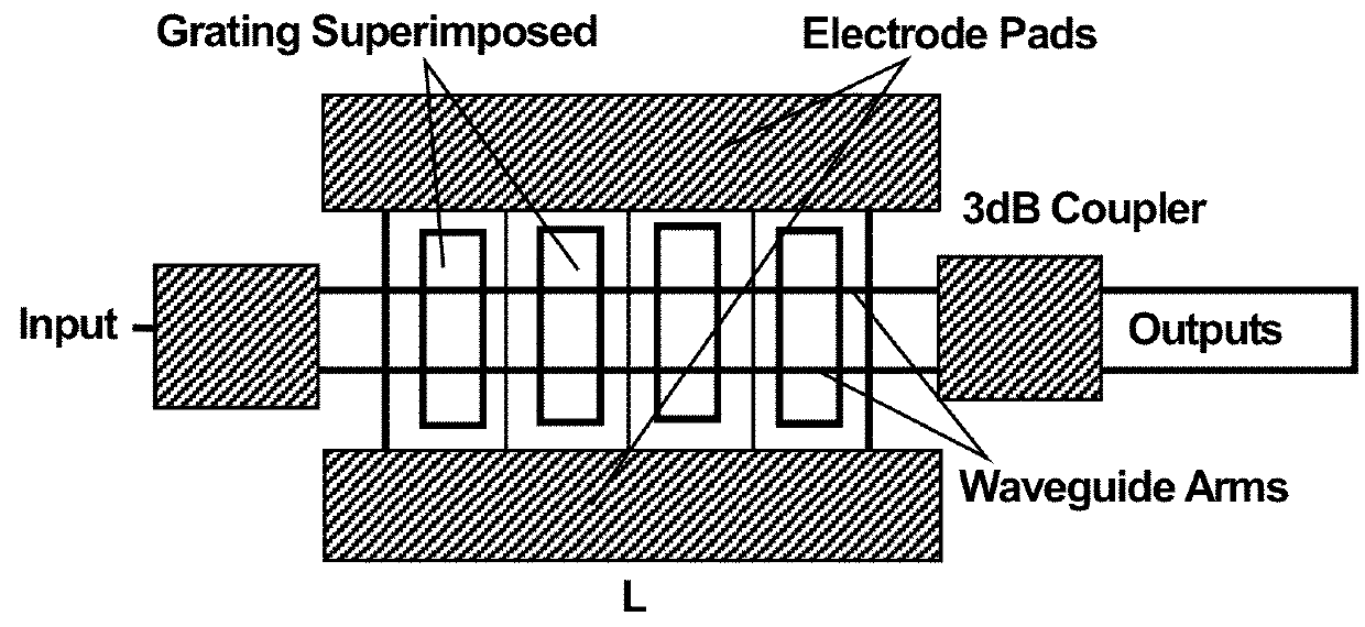
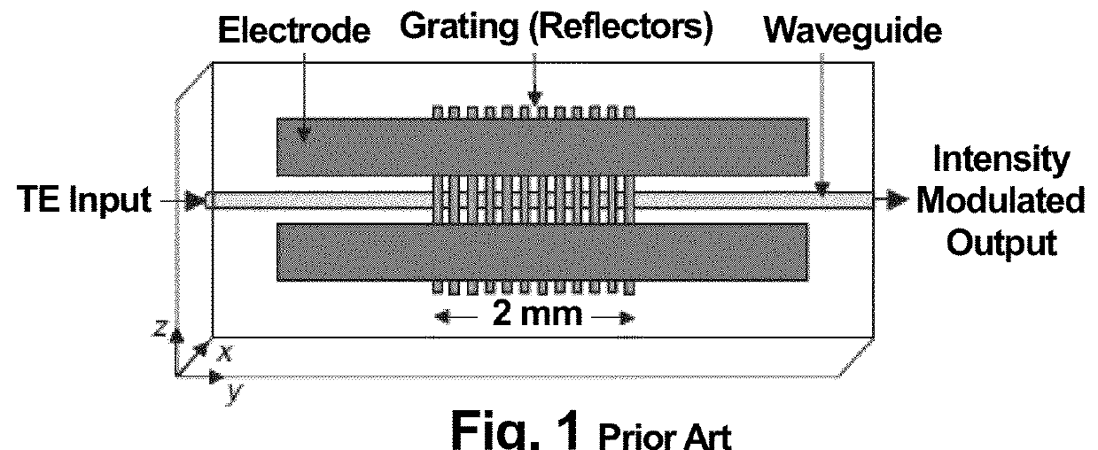
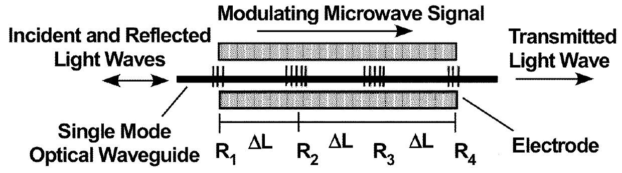
[0039]The present invention relates to an optical-waveguide grating modulator that modulates the light passing through it. The modulator modulates the intensity of the light that is partially transmitted through and partially reflected by one or more gratings. The modulation of that light is controlled by a traveling RF electromagnetic (EM) field that propagates parallel to the directions of the transmitted and reflected light and co-propagates with the transmitted light. The optical waveguide grating is fabricated in an electro-optic material whose optical refractive index depends on the electric-field component of the traveling RF field. When the material's optical refractive index is modulated by the time-varying RF field (the input RF signal), the transmission / reflection spectrum of the grating is shifted accordingly, along the frequency (or wavelength) axis. This changes the net transmission or reflection of the various frequency components of the light.

[0040]The disclosed modu...


PUM

PropertyMeasurementUnit
dielectric constantaaaaaaaaaa
sizeaaaaaaaaaa
sizeaaaaaaaaaa

Abstract

An optical-waveguide grating modulator is compatible with high-frequency electrical modulation signals of limited bandwidth. The modulator comprises an optical grating formed in an optical waveguide constructed from electro-optic (EO) material and an electrode that is an RF waveguide or RF transmission line that conducts a traveling-wave electromagnetic (EM) field and that contains a portion of the optical-grating waveguide with a continuous grating. The RF input modulation signal is coupled into an RF EM field that propagates through the RF waveguide or transmission line in a direction that is parallel to the direction the light propagates in the optical-grating waveguide and that EM field overlaps the optical-grating waveguide. The light travels along the optical-grating waveguide preferably at the same velocity as the RF EM field travels along the RF waveguide or transmission line.

Description

CROSS REFERENCE TO RELATED APPLICATIONS[0001]This application is related to U.S. Pat. No. 7,835,600 issued Nov. 16, 2010 and entitled “Microwave Receiver Front-End Assembly and Array” the disclosure of which is hereby incorporated herein by reference. This application is also related to U.S. patent application Ser. No. 12 / 239,980 by Oleg Efimov filed Sep. 22, 2008.TECHNICAL FIELD[0002]This disclosure relates to an optoelectronic modulator for use in RF photonic links and more particularly of an electro-optic grating modulator with velocity matched traveling-wave electrodes.BACKGROUND[0003]Optical or photonic links that comprise a laser, an optoelectronic modulator and a photodetector are known in the realm of RF photonics.[0004]A prior art grating intensity modulator is described in an article by R. Kim et al. (Electronics Letters, vol. 41, no. 18, 1 Sep. 2005) and is illustrated in FIG. 1. This modulator has a bulk electrode in which the RF signal is applied to the electrode as a w...

Claims


Application Information

Patent Timeline
Patent Type & Authority Patents(United States)
IPC IPC(8): G02F1/01G02F1/035G02F1/065
CPCG02F1/011G02F1/0356G02F1/065G02F2201/127G02F2201/307
Inventor YAP, DANIELEFIMOV, OLEG M.SCHAFFNER, JAMES H.
Owner HRL LAB
Why Eureka
Try Eureka