Three-dimensional integrated circuit stack

a technology of integrated circuits and stacks, applied in the direction of electrical equipment, semiconductor devices, semiconductor/solid-state device details, etc., can solve the problems of increasing wire resistance, reducing the cross-sectional area correspondingly, and limiting the performance of many integrated circuits, so as to achieve the effect of limiting benefits and over-all length of wires used to route signals

Active Publication Date: 2016-05-10
QUALCOMM INC
View PDF9 Cites 2 Cited by
  • Summary
  • Abstract
  • Description
  • Claims
  • Application Information

AI Technical Summary

Benefits of technology

[0004]To overcome the influence of wire resistance on integrated circuit performance, overall length of wires used to route signals (e.g., current or voltage) between the electronic devices of the integrated circuit may be shortened. Shortening wire traces between the electronic devices can be done by spacing electronic device closer together in the integrated circuit; however, manufacturing and design constraints can limit benefits that can be achieved by adjusting spacing.

Problems solved by technology

As integrated circuit and electronic device sizes have decreased and low power / high speed operation have become more important, some circuit characteristics have become more limiting.
However, since the number of electronic devices in each integrated circuit has continued to increase, there has not been a corresponding decrease in wire length to offset the decrease in cross sectional area.
Accordingly, wire resistance has become an increasingly important limitation on performance of many integrated circuits.
Shortening wire traces between the electronic devices can be done by spacing electronic device closer together in the integrated circuit; however, manufacturing and design constraints can limit benefits that can be achieved by adjusting spacing.
However, traditional wiring schemes can limit benefits that can be gained by modified wire routing.
For example, due to manufacturing constraints, very large scale integrated circuits often use Manhattan wiring schemes (also referred to as “taxicab routing”) to interconnect circuit devices.
However, for very small wire widths, adding metal layers with diagonal (relative to a Manhattan wiring scheme) wires can give rise to considerable manufacturing difficulties, such as alignment and multiple patterning and / or multiple exposure complications.

Method used


Image

  • Three-dimensional integrated circuit stack
  • Three-dimensional integrated circuit stack
  • Three-dimensional integrated circuit stack

Examples


Embodiment Construction

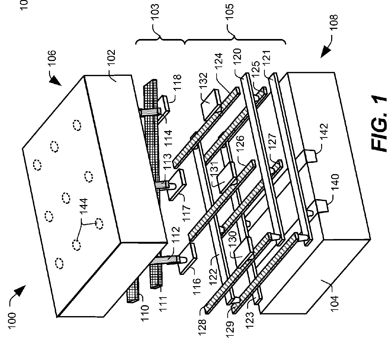
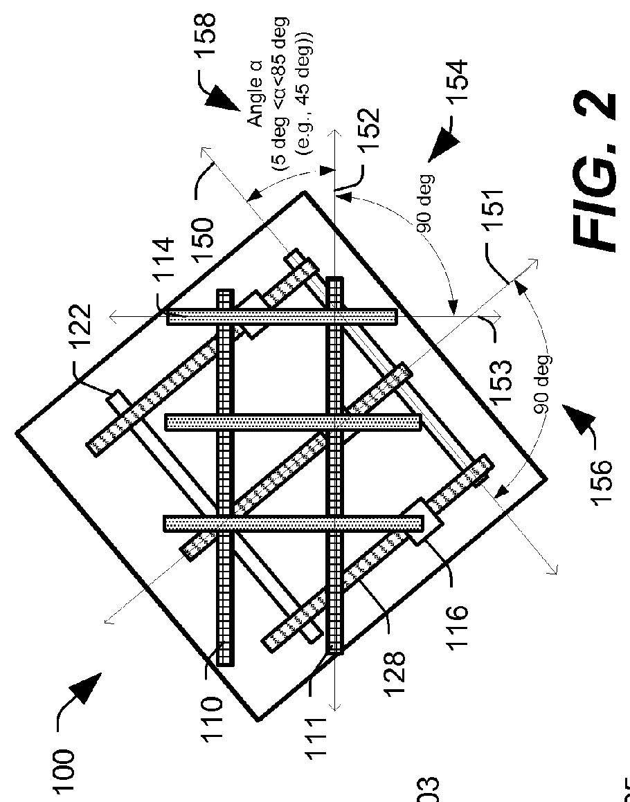
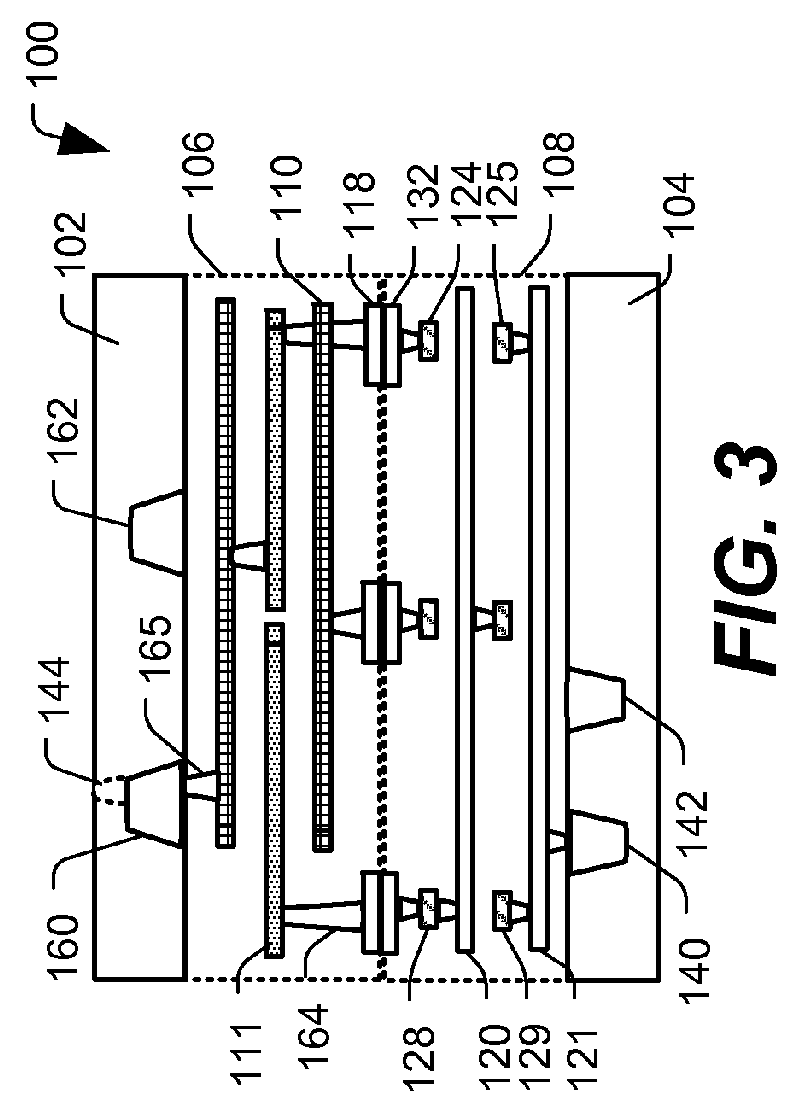
[0028]FIGS. 1, 2, and 3 illustrate a particular embodiment of a three-dimensional (3D) integrated circuit (IC) stack 100 that includes a first die 106 and a second die 108. FIG. 1 illustrates a perspective view of the first die 106 separate from the second die 108. FIG. 2 illustrates a top view of wiring of the first die 106 and wiring of the second die 108. FIG. 3 illustrates a cross sectional view of the first die 106 and the second die 108 in contact to form the 3D IC stack 100.

[0029]In FIGS. 1-3, certain components have been omitted to highlight the arrangement of the wires of the dies 106, 108. For example, dielectric separating the wires of the dies 106, 108 has been omitted. Additionally, only a few representative electronic devices and a few representative vias have been illustrated. The specific arrangement and number of wiring layers, vias, and electronic devices in particular embodiments will depend on specific circuit and design goals. For example, in a particular embodi...


PUM


Abstract

A particular three-dimensional integrated circuit stack includes a first die including a first bonding interface and a first plurality of interconnect layers arranged according to a first Manhattan wiring scheme. The three-dimensional integrated circuit stack also includes a second die including a second bonding interface and a second plurality of interconnect layers arranged according to a second Manhattan wiring scheme. The first die and the second die stacked with the first bonding interface coupled to the second bonding interface such that the first Manhattan wiring scheme and the second Manhattan wiring scheme are non-Manhattan with respect to each other.

Description

I. FIELD[0001]The present disclosure is generally related to three-dimensional integrated circuit stacks.II. DESCRIPTION OF RELATED ART[0002]Advances in technology have resulted in smaller and more powerful computing devices. For example, there currently exist a variety of portable personal computing devices, including wireless telephones such as mobile and smart phones, tablets and laptop computers that are small, lightweight, and easily carried by users. These devices can communicate voice and data packets over wireless networks. Further, many such devices incorporate additional functionality such as a digital still camera, a digital video camera, a digital recorder, and an audio file player. Also, such devices can process executable instructions, including software applications, such as a web browser application, that can be used to access the Internet. As such, these devices can include significant computing capabilities.[0003]Additionally, advances in technology have enabled ma...

Claims


Application Information

Patent Timeline
Patent Type & Authority Patents(United States)
IPC IPC(8): H01L23/48H01L23/528H01L27/06H01L23/00
CPCH01L23/5283H01L27/0688H01L23/481H01L24/82H01L23/528H01L25/0657G06F30/394
Inventor YI, WEILOU, YIPENZES, PAULSRIVASTAVA, PRANJAL
Owner QUALCOMM INC
Why Eureka
Try Eureka