High speed processing unit with non-volatile register

a processing unit and register technology, applied in the field of high-speed processing units with non-volatile registers, can solve the problems of difficult to increase the memory capacity of the register, and achieve the effects of high reliability, low power consumption, and significant capacity of the non-volatile register

Active Publication Date: 2016-05-17
SEMICON ENERGY LAB CO LTD
View PDF142 Cites 3 Cited by
  • Summary
  • Abstract
  • Description
  • Claims
  • Application Information

AI Technical Summary

Benefits of technology

[0009]With an enriched infrastructure of the information communication means, an improvement in the information-processing capability and an increase in the continuous operation time of a portable information terminal have been strongly requested. Also in terms of energy problems, a reduction in the power consumption of a processing unit has been requested.
[0010]In order to improve the processing speed of a processing unit, a memory circuit needs to be provided such that access to data in an arithmetic portion is easy. For example, the number of registers (in other words, the memory capacity of the memory circuit) is increased.

Problems solved by technology

However, it has been difficult to increase the memory capacity of the register while power consumption is reduced because most memory circuits operating at high speed are volatile and thus consume power constantly for storing data.

Method used


Image

  • High speed processing unit with non-volatile register
  • High speed processing unit with non-volatile register
  • High speed processing unit with non-volatile register

Examples


embodiment 1

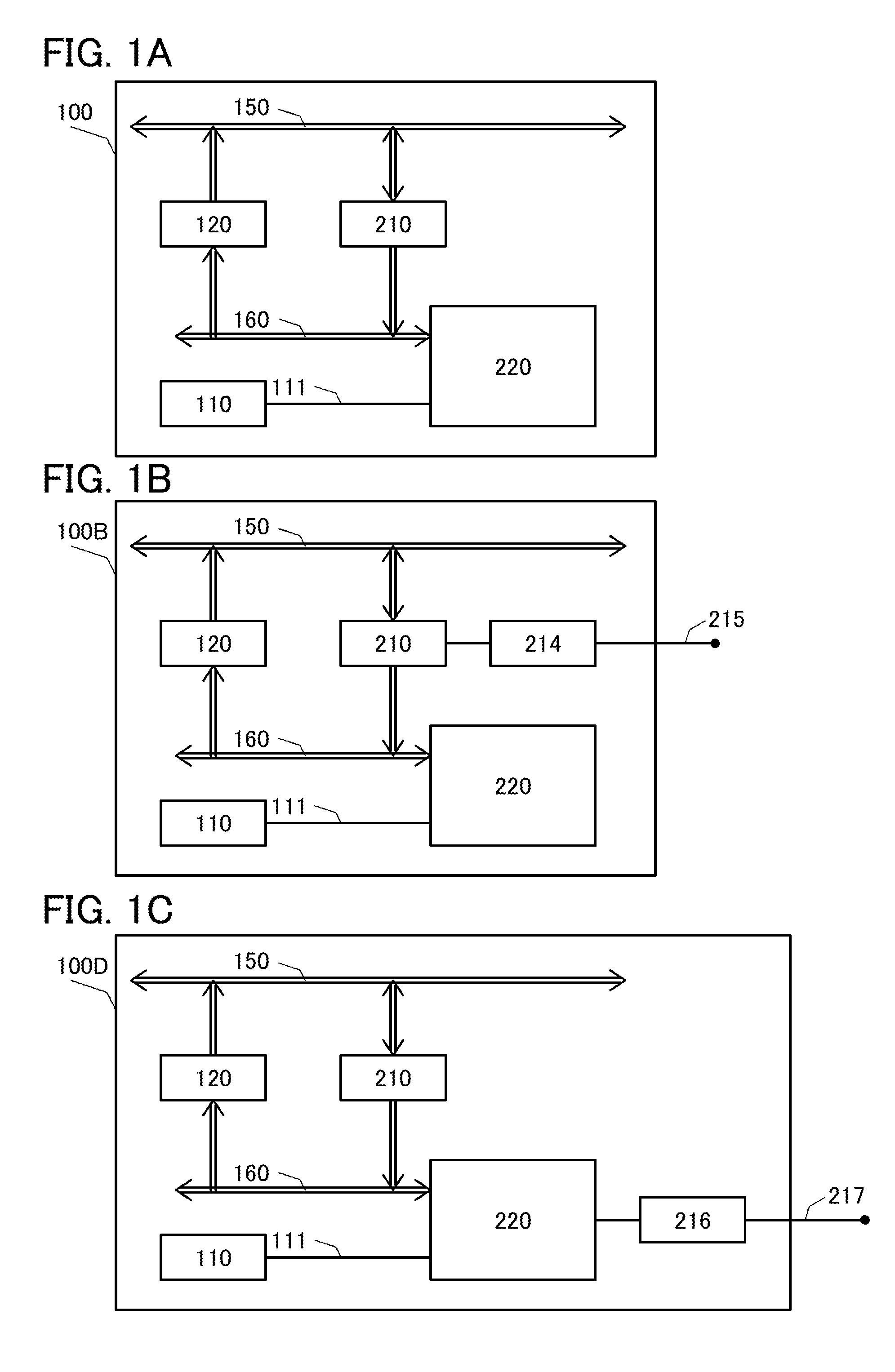
[0057]In this embodiment, the structure of a semiconductor device of one embodiment of the present invention will be described with reference to FIGS. 1A to 1C. FIG. 1A is a block diagram illustrating the structure of a semiconductor device of one embodiment of the present invention, FIG. 1B is a block diagram illustrating the structure of a semiconductor device of another embodiment of the present invention, and FIG. 1C is a block diagram illustrating the structure of a semiconductor device of yet another embodiment of the present invention.

[0058]The semiconductor device illustrated in FIG. 1A includes a register 210 electrically connected to a first transmission path 150 and a second transmission path 160, a reading / writing circuit 120 electrically connected to the first transmission path 150 and the second transmission path 160, a nonvolatile FILO register 220 electrically connected to the second transmission path 160, a control circuit 110 controlling the nonvolatile FILO regist...

modification example 1

[0073]A modification example of the semiconductor device described in this embodiment of the present invention will be described with reference to FIG. 1B.

[0074]A semiconductor device 100B illustrated in FIG. 1B includes a first memory access determination circuit 214 which outputs a wait signal in a period during which data is written to the nonvolatile FILO register 220.

[0075]Since the semiconductor device 100B includes the first memory access determination circuit 214, a failure in which, before writing data read from the register 210 to the nonvolatile FILO register 220 is finished, another data is written to the register 210 can be prevented. As a result, a semiconductor device with less malfunction, high reliability, and low power consumption, which includes a register from which data can be stored at high speed, can be provided.

[0076]A memory access determination circuit that can be used in the modification example of this embodiment will be described below.

>

[0077]The first m...

modification example 2

[0078]Another modification example of the semiconductor device described in this embodiment of the present invention will be described with reference to FIG. 1C.

[0079]A semiconductor device 100D illustrated in FIG. 1C includes a second memory access determination circuit 216 which outputs a wait signal in a period during which data is written to the nonvolatile FILO register 220.

[0080]Since the semiconductor device 100D includes the second memory access determination circuit 216, data which is read from the register 210 and then written to the nonvolatile FILO register 220 is monitored so that a flood of data can be prevented. As a result, a semiconductor device with less malfunction, high reliability, and low power consumption, which includes a register from which data can be stored at high speed, can be provided.

[0081]The second memory access determination circuit 216 that can be used in the modification example of this embodiment will be described below.

>

[0082]The second memory a...


PUM


Abstract

A semiconductor device in which the power consumption of a register is low is provided. Further, a processing unit whose operation speed is high and whose power consumption is low is provided. In the semiconductor device, a register operating at high speed and a nonvolatile FILO (first-in-last-out) register capable of reading and writing data from / to the register are provided.

Description

BACKGROUND OF THE INVENTION[0001]1. Field of the Invention[0002]The present invention relates to an object, a method, or a manufacturing method. Further, the present invention relates to a process, a machine, manufacture, or a composition of matter. In particular, the present invention relates to, for example, a semiconductor device, a display device, a light-emitting device, a power storage device, a driving method thereof, or a manufacturing method thereof. In particular, the present invention relates to a semiconductor device including a register and a processing unit including the semiconductor device.[0003]2. Description of the Related Art[0004]The processing speed of a processing unit is significantly affected by the speed at which an arithmetic portion accesses data (the speed of reading operation and writing operation). For that reason, the processing unit is provided with a memory circuit called a register, which operates at high speed.[0005]The arithmetic portion needs to ...

Claims


Application Information

Patent Timeline
Patent Type & Authority Patents(United States)
IPC IPC(8): G11C7/22G11C7/00G11C19/08
CPCG11C7/00G11C19/0875
Inventor SHIONOIRI, YUTAKAKOBAYASHI, HIDETOMOKUROKAWA, YOSHIYUKI
Owner SEMICON ENERGY LAB CO LTD
Why Eureka
Try Eureka