Switching regulator and control circuit and control method therefor

a technology of switching regulator and control circuit, applied in the direction of electric variable regulation, process and machine control, instruments, etc., can solve the problems of different control effects on performance, low voltage ripple, and loss of control circuit using supplementary signals

Active Publication Date: 2016-05-17
SILERGY SEMICON TECH (HANGZHOU) CO LTD
View PDF8 Cites 4 Cited by
  • Summary
  • Abstract
  • Description
  • Claims
  • Application Information

AI Technical Summary

Benefits of technology

[0023]In the present disclosure, the control circuit generates a supplementary signal varying with state of the power stage in a first mode and keeps the supplementary signal substantially unchanged in a second mode with respect to the value at the moment of switching from the first mode to the second mode so that the value of the supplementary signal at the moment of mode switching is maintained substantially constant, therefore, a steady state is achieved quickly, and ripples in the output voltage are restrained.

Problems solved by technology

Thus, adopting different detection signals and / or control circuits may result in different control effects on performance.
However, control circuits using the supplementary signal would lose the control of the supplementary signal when the power stage switches to a large capacitance loaded or light loaded condition.
This results in that the voltage ripple may be at a high level.

Method used


Image

  • Switching regulator and control circuit and control method therefor
  • Switching regulator and control circuit and control method therefor
  • Switching regulator and control circuit and control method therefor

Examples


first embodiment

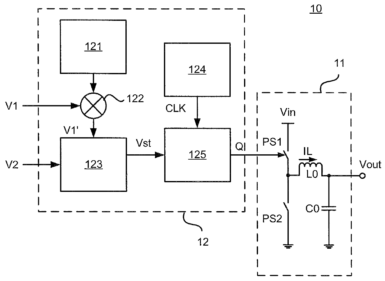
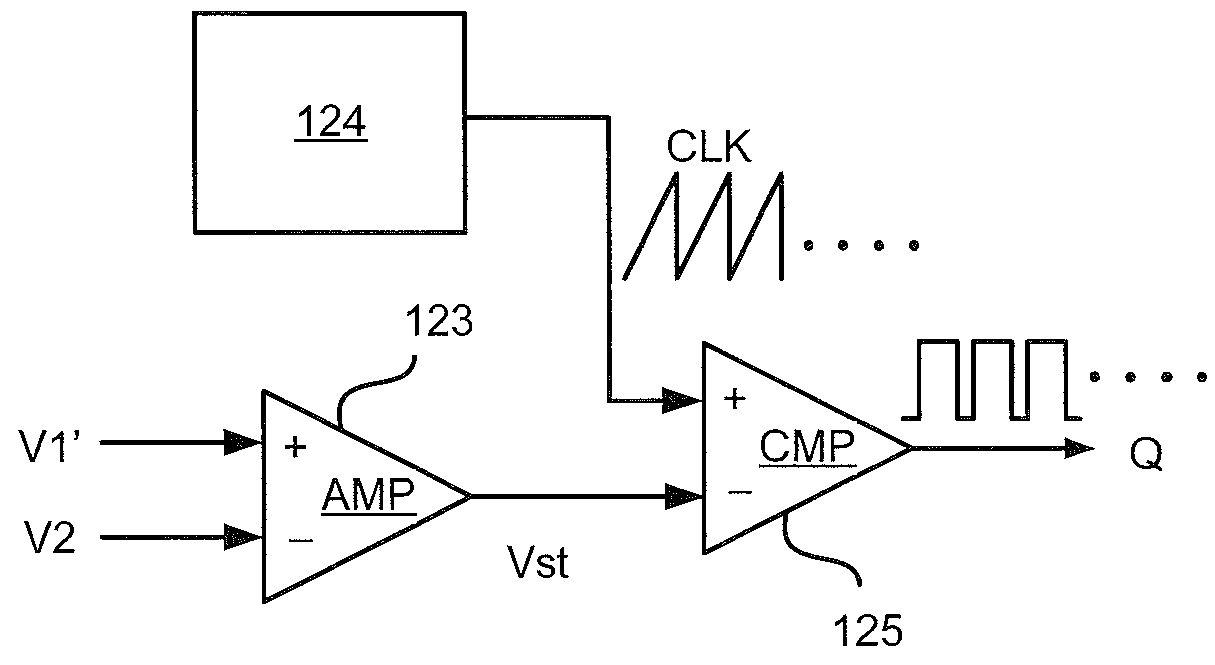
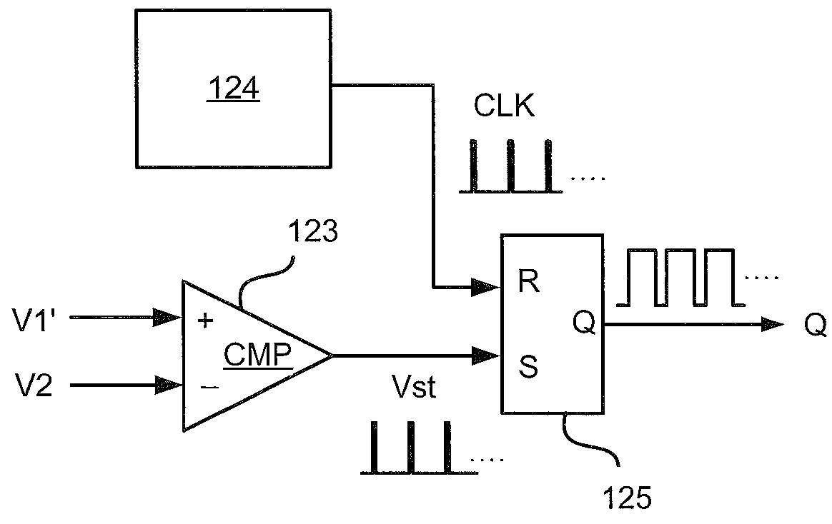
[0045]FIG. 1A is a schematic diagram of a switching regulator in accordance with the present disclosure. As shown in FIG. 1A, switching regulator 10 comprises power stage 11 and control circuit 12.

[0046]Power stage 11 comprises power switch PS1, rectifying element PS2, inductive element L0 and filtering element C0.

[0047]Wherein, power switch PS1 may be any controlled semiconductor switching device, such as Metal Oxide Semiconductor Field Effect Transistor (MOSFET), Insulated Gate Bipolar Transistor (IGBT) etc. Rectifying element PS2 is electrically coupled to power switch PS1. In the present embodiment, rectifying element PS2 may adopt a diode or any kind of controlled semiconductor switch such as Metal Oxide Semiconductor Field Effect Transistor (MOSFET), Insulated Gate Bipolar Transistor (IGBT) etc. Inductive element L0 is electrically coupled to power switch PS1 which switches between states of storing energy and releasing energy with on and off of power switch PS1. Inductive ele...

second embodiment

[0065]FIG. 2A is a schematic diagram of a switching regulator in accordance with the present disclosure. As shown in FIG. 2A, switching regulator 20 comprises power stage 21 and control circuit 22. Wherein, the power stage 21 is substantially the same as the power stage shown in FIG. 1A, and will not be illustrated hereinafter. It is to be understood by those skilled in the art that power stage 11 may adopt other well-known circuit topologies such as a boost topology and a buck-boost topology as necessary.

[0066]Control circuit 22 comprises supplementary signal generator 221, superimposing circuit 222, state detection circuit 223, clock generator 224 and switching control signal generator 225.

[0067]In the present embodiment, first signal V1 is feedback voltage Vfb, and second signal V2 is reference voltage Vref. Feedback Vfb is obtained from output voltage Vout of power stage 21.

[0068]The supplementary signal comprises ripple voltage Vr. Supplementary signal generator 221 is ripple g...

sixth embodiment

[0144]FIG. 6 is a schematic diagram of a switching regulator in accordance with the present disclosure. As shown in FIG. 6, switching regulator 60 comprises power stage 61 and control circuit 62. Wherein, power stage 61 is substantially the same as the power stage shown in FIG. 1A, and will not be illustrated hereinafter. It is to be understood by those skilled in the art that power stage 61 may adopt other well-known circuit topologies such as a boost topology and a buck-boost topology as necessary.

[0145]Control circuit 62 comprises supplementary signal generator 621, superimposing circuit 622, state detection circuit 623, clock generator 624 and switching control signal generator 625.

[0146]In the present embodiment, first signal V1 is reference voltage Vref, and second signal V2 is feedback voltage Vfb. Wherein the supplementary signal comprises correction voltage Vcorr. Correction voltage Vcorr is configured to correct or compensate reference voltage Vref so that a reference volt...


PUM


Abstract

Disclosed are a switching regulator and a control circuit and a control method therefor. In one embodiment, the control circuit generates a supplementary signal varying with a state parameter of the power stage in a first mode and keeps the supplementary signal substantially unchanged in a second mode with respect to the value thereof at the moment of switching from the first mode to the second mode so that the supplementary signal at the moment of mode switching is maintained substantially constant, therefore, a steady state can be achieved quickly, and ripples in the output voltage are restrained.

Description

CLAIM OF PRIORITY AND CROSS-REFERENCE TO RELATED APPLICATION(S)[0001]This application claims the benefit of Chinese Patent Application No. 201310731190.X, filed on Dec. 26, 2013, which is incorporated herein by reference in its entirety.BACKGROUND OF THE INVENTION[0002]1. Field of the Invention[0003]The present invention relates to the field of power electronics, and particularly to a switching regulator and a control circuit and a control method therefor.[0004]2. Description of the Related Art[0005]A switching regulator typically comprises a power stage and a control circuit. The control circuit can consider variations in an input voltage, internal parameters and external loads, and can regulate the ratio of on / off time of the switch system in the power stage, so that an output voltage or an output current of the switching regulator can be maintained as substantially constant. Therefore, the design of a particular control circuitry and approach is very important to the overall perf...

Claims


Application Information

Patent Timeline
Patent Type & Authority Patents(United States)
IPC IPC(8): G05F1/00H02M3/156H02M1/00
CPCH02M3/156H02M2001/0032Y02B70/16H02M1/14H02M1/0032Y02B70/10
Inventor YUAN, XIAOLONG
Owner SILERGY SEMICON TECH (HANGZHOU) CO LTD
Why Eureka
Try Eureka