Check patentability & draft patents in minutes with Patsnap Eureka AI!

Digital-to-time converter

a converter and digital technology, applied in the field of data converters, can solve the problems of reducing the usefulness of data communication applications to support significantly lower data rates, affecting the performance of jitter, and affecting the quality of data communication applications

Active Publication Date: 2016-06-07
SILICON LAB INC
View PDF18 Cites 39 Cited by
  • Summary
  • Abstract
  • Description
  • Claims
  • Application Information

AI Technical Summary

Benefits of technology

The patent describes an apparatus and method for a digital-to-time converter that can change the time delay of an input signal based on a digital code. This allows for precise synchronization of signals in electronic devices. The apparatus includes a digital-to-analog signal converter and a switch to selectively connect the input signal to a reference signal. The method involves establishing a specific voltage level on the input node and changing the voltage thereon based on the digital code. The output signal is generated based on the comparison of the voltage on the input node to a switching threshold voltage level. The apparatus and method can be used in clock synthesizers and feedback loops of phase-locked loops. The technical effect is improved precision and accuracy in signal synchronization.

Problems solved by technology

The analog quantization error of the dithering noise-shaped integer control signal causes substantial deterministic jitter that dominates the jitter performance.
As a result, the system is more dependent on voltage-controlled oscillator phase noise performance which can often translate into higher power consumption.
In addition, the low loop bandwidth of the clock synthesizer reduces its usefulness in data communication applications to supporting significantly lower data rates than might otherwise be desired.
However, an input integer divider provides frequency resolution at the expense of phase noise.
As the frequencies of ckin and ckout increase, the target clock period decreases and jitter introduced by the digital-to-time converter circuits become a larger fraction of the target clock period, thereby causing output clock signals from conventional clock synthesizer designs to fail to meet target performance specifications.

Method used


Image

  • Digital-to-time converter
  • Digital-to-time converter
  • Digital-to-time converter

Examples


Embodiment Construction

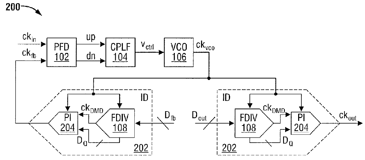
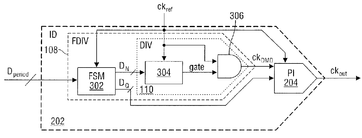
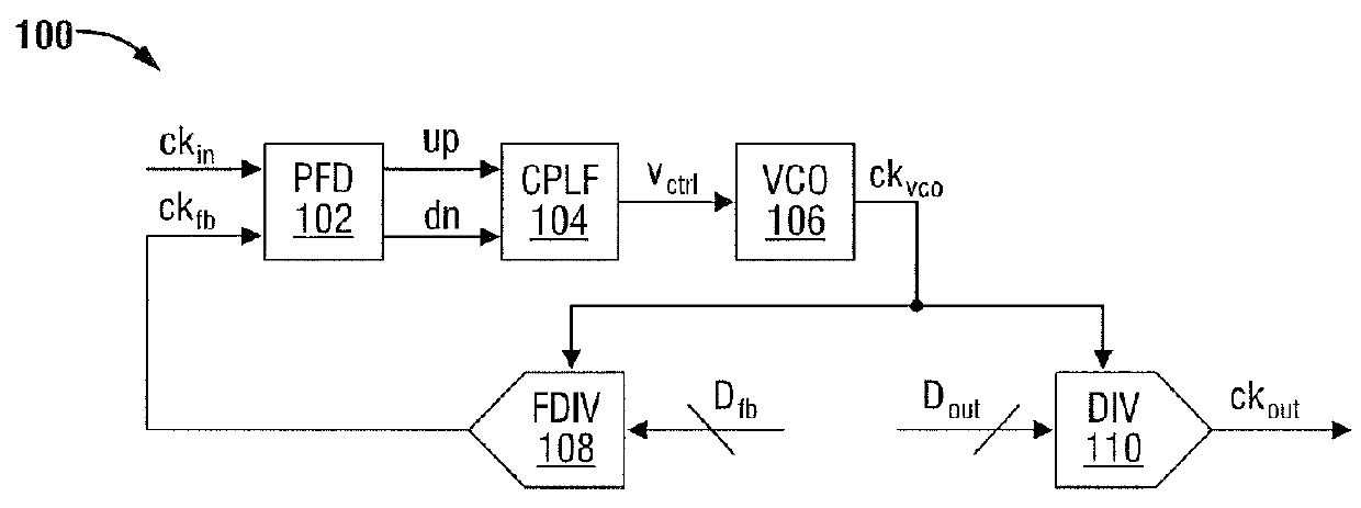
[0012]In at least one embodiment of the invention, an apparatus includes a digital-to-time converter. The digital-to-time converter includes a first node, a second node configured to receive a reference signal, and a digital-to-analog signal converter configured to couple a passive impedance to the first node. The passive impedance is selected according to the digital code. The digital-to-time converter also includes a first switch configured to selectively couple the first node to a second reference signal in response to an input signal and a comparator configured to generate the output signal based on a first signal on the first node and the reference signal on the second node. Edges of the output signal may correspond to the input signal edges linearly delayed based on the digital code. The digital-to-time converter may include a second switch configured to selectively couple the first node to a third reference signal in response to a first control signal. The first node may be c...


PUM


Abstract

A digital-to-time converter includes a first node, a second node configured to receive a reference signal, and a digital-to-analog signal converter configured to couple a passive impedance to the first node. The passive impedance is selected according to the digital code. The digital-to-time converter also includes a first switch configured to selectively couple the first node to a second reference signal in response to the input signal and a comparator configured to generate the output signal based on a first signal on the first node and the reference signal on the second node. The digital-to-time converter may include a second switch configured to selectively couple the first node to a third reference signal in response to a first control signal.

Description

BACKGROUND[0001]1. Field of the Invention[0002]The present invention is related to data converters and more particularly to digital-to-analog converters.[0003]2. Description of the Related Art[0004]In general, a digital-to-time converter is a digital-to-analog data converter that generates an output signal having a period or edge delay based on a digital control word and a reference clock signal. For example, a clock divider circuit is a digital-to-time period converter that generates an output clock signal based on a reference clock signal and a digital control word indicating a divide ratio (e.g. an integer divide ratio or a fractional divide ratio). The analog output is the period of the output clock signal. The output clock period is based on the digital control word and the clock period of the reference clock signal. The output clock signal has a digitally-defined, full-scale range and a least-significant bit clock period.[0005]A typical integer clock frequency divider is a dig...

Claims


Application Information

Patent Timeline
IPC IPC(8): H03M1/82H03M1/66H03M1/08H03M1/10H03K5/135
CPCH03M1/1033H03M1/0836H03M1/66H03K5/135H03M1/82
Inventor CAFFEE, AARON J.DROST, BRIAN G.
Owner SILICON LAB INC
Features
  • R&D
  • Intellectual Property
  • Life Sciences
  • Materials
  • Tech Scout
  • Unparalleled Data Quality
  • Higher Quality Content
  • 60% Fewer Hallucinations
Learn More