Fiber optic coupler array

a fiber optic coupler and array technology, applied in the field of waveguide can solve the problems of not being suitable for large-spectral bandwidth optical coupling, putting a stringent demand on the alignment of fiber both vertically and the input and output couplers

Active Publication Date: 2016-06-28
UNIV OF CONNECTICUT +1
View PDF27 Cites 14 Cited by
  • Summary
  • Abstract
  • Description
  • Claims
  • Application Information

AI Technical Summary

Benefits of technology

[0014]The photonic IC can be realized with a material system of group III-V materials. The photonic IC can also be realized from an epitaxial layer structure that includes an n-type modulation doped quantum well interface offset vertically from a p-type modulation doped quantum well interface.

Problems solved by technology

Waveguide input and output couplers have always been an important issue in optical integrated circuit design.
The drawbacks are that the diffractive nature of this approach relies on interferometric behavior applicable only to a limited wavelength range and therefore may not be suitable for large-spectral bandwidth optical coupling.
While the lateral coupling has weak polarization dependence and is insensitive to the input bandwidth, it puts a stringent demand on the alignment of the fiber both vertically and laterally.
Also, SSC designs require excellent control of the critical dimensions and lensed fiber or special fiber are often needed for nano-waveguides especially when implemented for short wavelength, which adds to the cost and complicates the fabrication and packaging of the integrated circuits.

Method used


Image

  • Fiber optic coupler array
  • Fiber optic coupler array
  • Fiber optic coupler array

Examples


Embodiment Construction

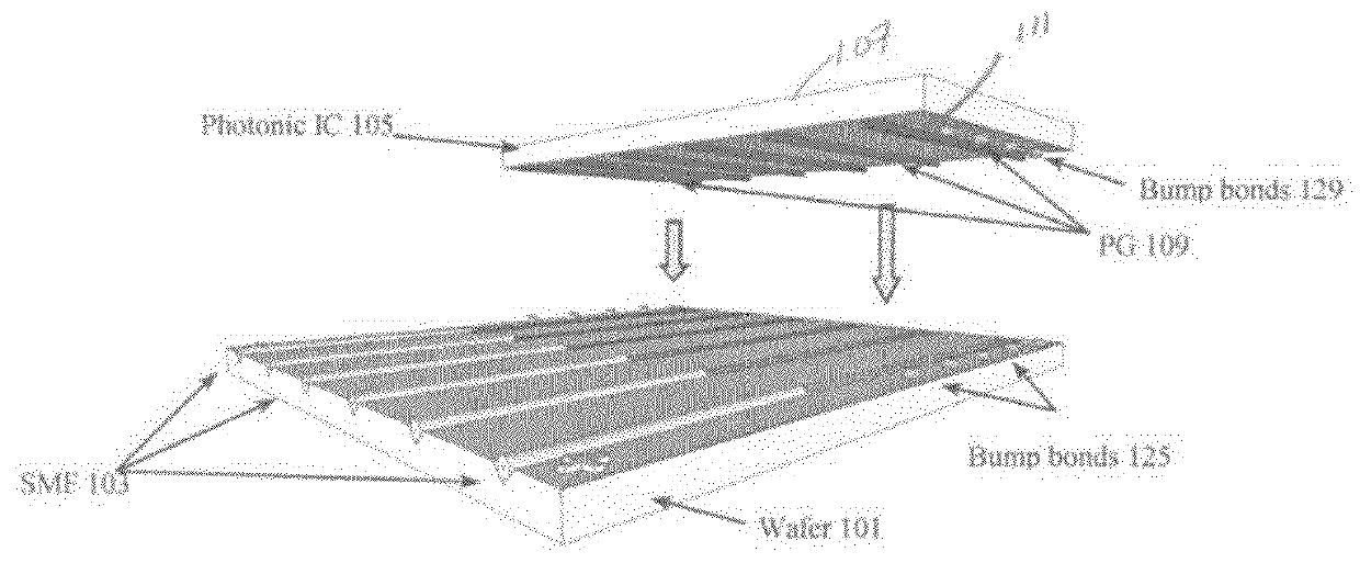
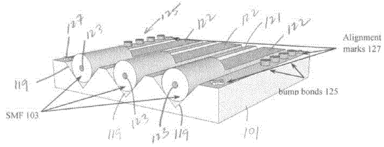
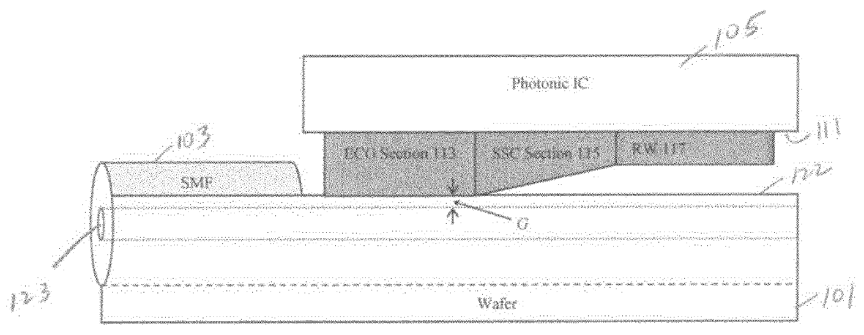
[0027]FIG. 1 illustrates a fiber optic coupler array 100 according to the present application. The coupler array 100 includes two parts: a wafer 101 that mechanically supports a plurality of single-mode optical fibers (SMFs) 103; and a photonic integrated circuit (IC) 105 with active electro-optical components that are operably coupled to the SMFs 103 supported by the wafer 101. The SMFs 103 can extend beyond the periphery of the wafer 101 for connection to other network components as needed. The photonic IC 105 is configured in an inverted configuration (with the substrate 107 up) with on-chip passive semiconductor waveguides (PG) 109 integral to its top surface 111 (opposite the substrate 107). Each PG 109 is configured such that is in intimate contact with a corresponding SMF 103 in which the fiber cross-section has been suitably modified to provide evanescent-wave coupling between the SMF 103 and the PG 109. As best shown in FIGS. 3 and 6, each PG 109 includes an evanescent coup...


PUM


Abstract

An assembly includes optical fibers each having a waveguide core, a photonic integrated circuit (IC) that includes in-plane waveguides corresponding to the optical fibers, and a substrate bonded to the photonic IC with grooves that support the optical fibers. The substrate and photonic IC can have metal bumps that cooperate to provide mechanical bonding and electrical connections between the substrate and photonic IC. Portions of the optical fibers supported by the substrate grooves can define flat surfaces spaced from the optical fiber cores. The photonic IC can include passive waveguide structures with a first coupling section that interfaces to the flat surface of a corresponding optical fiber (for evanescent coupling of optical signals) and a second coupling section that interfaces to a corresponding in-plane waveguide (for adiabatic spot-size conversion of optical signals).

Description

CROSS-REFERENCE TO RELATED APPLICATIONS[0001]The present application claims priority from U.S. Provisional Appl. No. 61 / 736,768, filed on Dec. 13, 2012 , herein incorporated by reference in its entirety.BACKGROUND[0002]1. Field[0003]The present application is related to waveguide input and output couplers for optical integrated circuits.[0004]2. State of the Art[0005]Waveguide input and output couplers have always been an important issue in optical integrated circuit design. Various coupling schemes have been proposed or demonstrated to overcome the low coupling efficiency between the optical fiber and the waveguides on the chip. Based on the direction at which light is coupled in or out of the waveguides, these schemes fall into one of two categories: vertical coupling (out of plane) and lateral coupling (in plane).[0006]Vertical coupling is typically accomplished with diffractive gratings incorporated into a waveguide layer to provide a conversion between the optical mode in the s...

Claims


Application Information

Patent Timeline
Patent Type & Authority Patents(United States)
IPC IPC(8): G02B6/30G02B6/42G02B6/122G02B6/14
CPCG02B6/305G02B6/1228G02B6/14G02B6/421G02B6/423G02B6/4249G02B6/4257
Inventor TAYLOR, GEOFF W.ZHANG, YAN
Owner UNIV OF CONNECTICUT
Why Eureka
Try Eureka