
Display device

a technology of display and film, applied in semiconductor devices, instruments, optics, etc., can solve problems such as display degradation, and achieve the effects of preventing moisture entry into the flattening film, enhancing the cover properties of the flattening film, and preventing display degradation

Active Publication Date: 2016-06-28
SHARP KK
View PDF21 Cites 1 Cited by
  • Summary
  • Abstract
  • Description
  • Claims
  • Application Information

AI Technical Summary

Benefits of technology

[0019]According to the first aspect of the present invention, since the protective film is provided on a flat surface, the covering properties of the flattening film are enhanced. Therefore, by covering the entire surface of the flattening film using the protective film having moisture-proof properties, the entry of moisture into the flattening film is prevented, enabling to prevent display degradation caused by moisture absorption of the flattening film.
[0020]According to the second aspect of the present invention, by disposing an edge surface of the flattening film within the region surrounded by the seal or under the seal, direct contact of the edge surface of the flattening film with air is prevented, enabling to more effectively prevent display degradation caused by moisture absorption of the flattening film.
[0021]According to the third aspect of the present invention, by forming an edge surface of the flattening film in a tapered shape, the covering properties of the edge surface of the flattening film are enhanced, enabling to more effectively prevent display degradation caused by moisture absorption of the flattening film.
[0022]According to the fourth aspect of the present invention, by also forming the moisture-proof protective film on a side surface of the contact portion, the number of moisture entry paths into the flattening film is reduced, enabling to more effectively prevent display degradation caused by moisture absorption of the flattening film.
[0023]According to the fifth aspect of the present invention, by sandwiching the protective film provided for moisture prevention by two electrodes, a capacitance is formed. The formed capacitance can be used as an auxiliary capacitance. In addition, by forming the two electrodes to be transparent electrodes, the auxiliary capacitance is allowed to have light transmission properties, enabling to increase the aperture ratio of a display element.
[0024]According to the sixth aspect of the present invention, by forming the first electrode in a slit shape, a fringing field can be produced. Therefore, in a liquid crystal display device, the alignment of a liquid crystal is controlled using the produced fringing field, by which viewing angle characteristics can be improved.

Problems solved by technology

However, when a liquid crystal display device is used under a high temperature and humidity environment, characteristics of a thin film transistor (hereinafter, referred to as a TFT) changes due to the influence of moisture that enters inside the device, which may cause display degradation.

Method used


Image

  • Display device
  • Display device
  • Display device

Examples


first embodiment

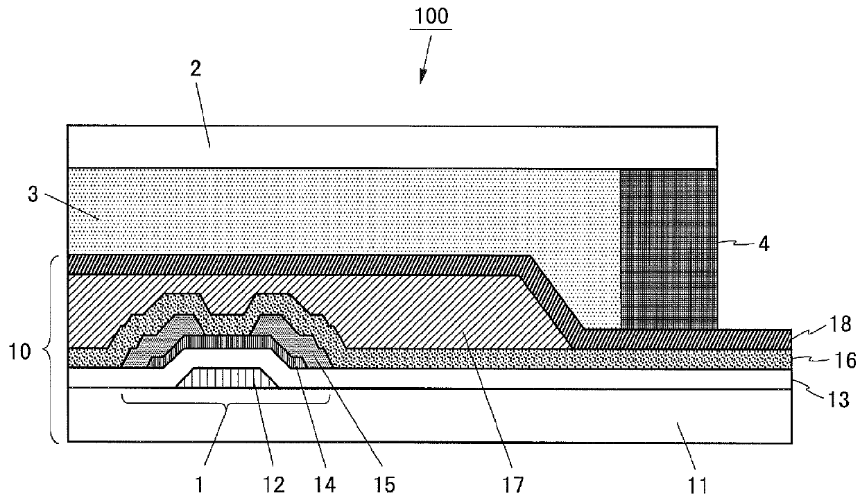
[0055]FIG. 1 is a cross-sectional view of a liquid crystal display device according to a first embodiment of the present invention. A liquid crystal display device 100 shown in FIG. 1 has a structure in which a TFT substrate 10 and a counter substrate 2 are bonded together and a liquid crystal 3 is filled between the two substrates. The TFT substrate 10 and the counter substrate 2 are disposed facing each other, and a seal 4 made of a resin is provided around a portion where the two substrates face each other. The counter substrate 2 is provided with a counter electrode, a color filter (none of which are shown), etc.

[0056]On the TFT substrate 10, a TFT 1 and various types of wiring lines (gate wiring lines, data wiring lines, etc.) are formed. The TFT 1 is formed by forming in turn a gate electrode 12, a gate insulating film 13, a semiconductor layer 14, and a source / drain electrode 15 on a glass substrate 11. On the substrate obtained after forming the TFT 1, a protective film 16, ...

second embodiment

[0076]FIG. 9 is a cross-sectional view of a liquid crystal display device according to a second embodiment of the present invention. A liquid crystal display device 200 shown in FIG. 9 has a structure in which a TFT substrate 20 and a counter substrate 2 are bonded together and a liquid crystal 3 is filled between the two substrates. Of the components in embodiments shown below, the same components as those in the aforementioned embodiment are denoted by the same reference characters and description thereof is omitted.

[0077]As in the first embodiment, the TFT substrate 20 of the liquid crystal display device 200 includes a pixel electrode provided on the opposite side of a protective film 18 from a flattening resin film 17; and a contact portion 5 that electrically connects the pixel electrode to a drain electrode 15 of a TFT 1. In the liquid crystal display device 100 according to the first embodiment, the protective film 18 is not formed on the side surfaces of the contact portion...

third embodiment

[0080]FIG. 10 is a cross-sectional view of a liquid crystal display device according to a third embodiment of the present invention. A liquid crystal display device 300 shown in FIG. 10 has a structure in which a TFT substrate 30 and a counter substrate 2 are bonded together and a liquid crystal 3 is filled between the two substrates.

[0081]On the substrate obtained after forming a gate insulating film 13, a common wiring line 31 to which a common voltage is applied is formed. A lower layer electrode 33 that is electrically connected to the common wiring line 31 is formed on a flattening resin film 17. A protective film 18 is formed to cover the entire surfaces of the flattening resin film 17 and the lower layer electrode 33. An upper layer electrode 32 that is electrically connected to a drain electrode 15 is formed on the protective film 18 so as to face the lower layer electrode 33 with the protective film 18 interposed therebetween. As such, the TFT substrate 30 includes the uppe...


PUM

PropertyMeasurementUnit
structureaaaaaaaaaa
tapered shapeaaaaaaaaaa
semiconductoraaaaaaaaaa

Abstract

A TFT 1 is formed on a glass substrate 11, and a flattening resin film 17 covering the TFT 1 is formed. Furthermore, a moisture-proof protective film 18 covering the entire surface of the flattening resin film 17 is formed. For the protective film 18, a SiO2 film, a SiN film, a SiON film, or a stacked film thereof is used. The edge surfaces of the flattening resin film 17 are disposed on the inner side of or under a seal 4, and are formed in a tapered shape. By this, the entry of moisture into the flattening resin film 17 is prevented, preventing display degradation. This effect becomes noticeable in a display device including an oxide semiconductor TFT.

Description

TECHNICAL FIELD[0001]The present invention relates to a display device such as a liquid crystal display device.BACKGROUND ART[0002]In recent years, liquid crystal display devices have been used in various fields and have been used under various environments. Liquid crystal display devices are also used, for example, under a high temperature and humidity environment. However, when a liquid crystal display device is used under a high temperature and humidity environment, characteristics of a thin film transistor (hereinafter, referred to as a TFT) changes due to the influence of moisture that enters inside the device, which may cause display degradation.[0003]FIG. 16 is a cross-sectional view of a conventional liquid crystal display device. The liquid crystal display device shown in FIG. 16 has a structure in which a TFT substrate 81 and a counter substrate 82 are bonded together and a liquid crystal 83 is filled between the two substrates. A seal 84 is provided around a portion where...

Claims


Application Information

Patent Timeline
Patent Type & Authority Patents(United States)
IPC IPC(8): G02F1/1333H01L29/786G02F1/1362G02F1/1339H01L27/12G02F1/1343G02F1/1368G02F1/1345
CPCG02F1/133345G02F1/1339G02F1/136277H01L29/78606G02F1/1345G02F1/1368G02F2001/133311G02F2001/133357G02F2001/134372G02F2201/501H01L27/1248H01L29/78636G02F1/133311G02F1/133357G02F1/134372G02F1/1333
Inventor MORIGUCHI, MASAOKANZAKI, YOHSUKETAKANISHI, YUDAIKUSUMI, TAKATSUGU
Owner SHARP KK
Learn More