Check patentability & draft patents in minutes with Patsnap Eureka AI!

Imaging lens, and electronic apparatus including the same

a technology of electronic equipment and optical lens, applied in the direction of optics, instruments, optics, etc., can solve the problems of unsuitable incorporation into mobile phones, digital cameras, etc., and achieve the effect of shortening the overall length and good optical performan

Active Publication Date: 2016-07-12
GENIUS ELECTRONICS OPTICAL CO LTD
View PDF21 Cites 0 Cited by
  • Summary
  • Abstract
  • Description
  • Claims
  • Application Information

AI Technical Summary

Benefits of technology

The design achieves a significant reduction in system length while maintaining good optical performance, including low spherical aberration and chromatic aberration, and is suitable for integration into portable electronic devices.

Problems solved by technology

The conventional imaging lens disclosed in U.S. Patent application Publication No. 20110316969 has a length greater than 14 mm, which renders it unsuitable to be incorporated into a mobile phone, a digital camera and / or other portable electronic devices with a thin design.

Method used


Image

  • Imaging lens, and electronic apparatus including the same
  • Imaging lens, and electronic apparatus including the same
  • Imaging lens, and electronic apparatus including the same

Examples


Embodiment Construction

[0058]Before the present invention is described in greater detail, it should be noted that like elements are denoted by the same reference numerals throughout the disclosure.

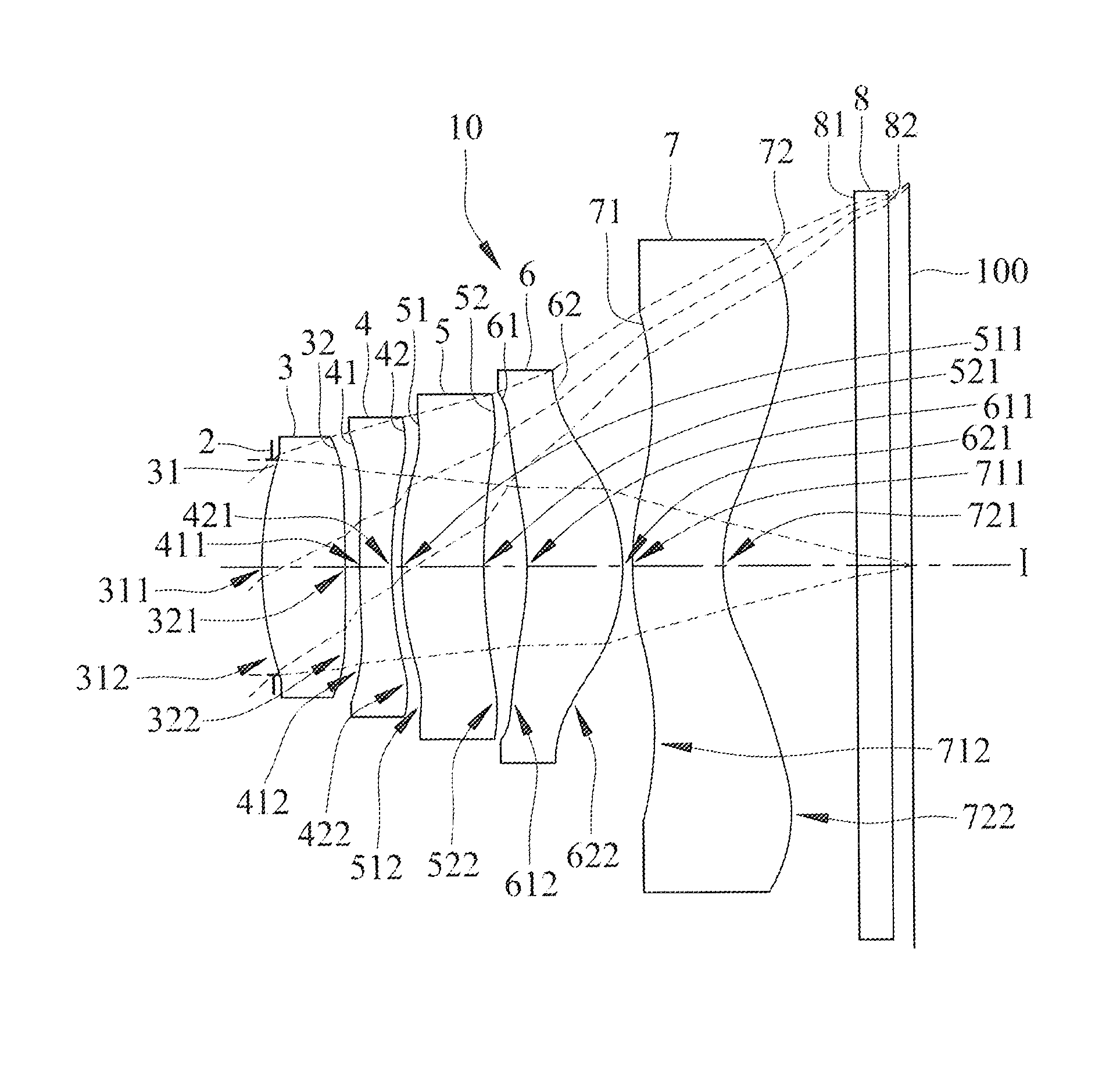
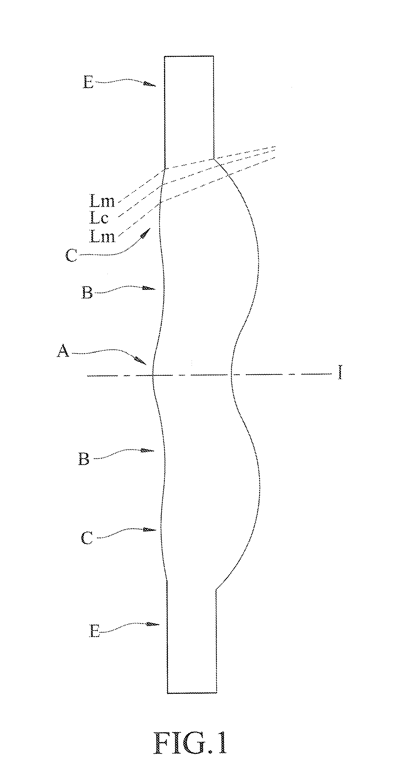
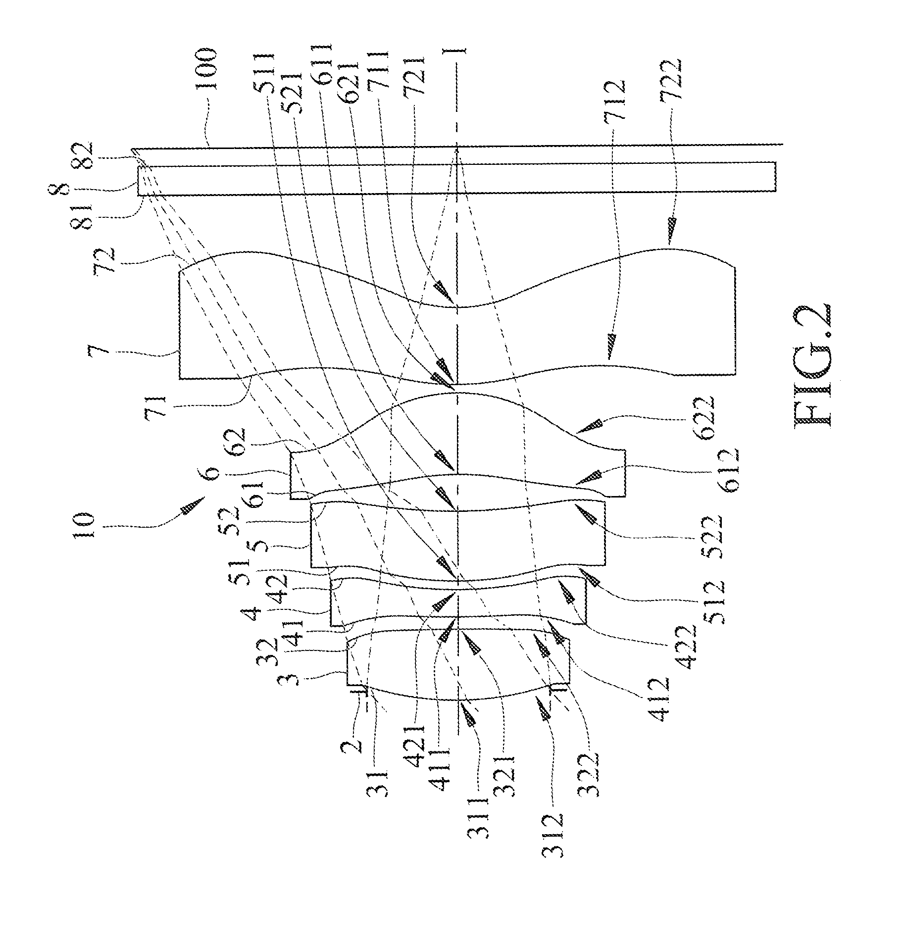
[0059]In the following description, “a lens element has a positive (or negative) refractive power” means the lens element has a positive (or negative) refractive power in a vicinity of an optical axis thereof. “An object-side surface (or image-side surface) has a convex (or concave) portion at a certain area” means that, compared to a radically exterior urea adjacent to said certain area, said certain area is more convex (or concave) in a direction parallel to the optical axis. Referring to FIG. 1 as an example, the lens element is radially symmetrical with respect to an optical axis (I) thereof. The object-side surface of the lens element has a convex portion at an area A, a concave portion at an area B, and a convex portion at an area C. This is because the area A is more convex in a direction parallel to the ...


PUM


Abstract

An imaging lens includes first to fifth lens elements arranged from an object side to an image side in the given order. Through designs of surfaces of the lens elements and relevant lens parameters, a short system length of the imaging lens may be achieved while maintaining good optical performance.

Description

CROSS-REFERENCE TO RELATED APPLICATION[0001]This application claims priority of Chinese Patent application No. 201410084670.6, filed on Mar. 10, 2014.BACKGROUND OF THE INVENTION[0002]1. Field of the Invention[0003]The present invention relates to an imaging lens and en electronic apparatus including the same.[0004]2. Description of the Related Art[0005]In recent years, as use of portable electronic devices (e.g., mobile phones and digital cameras) becomes ubiquitous, much effort has been put into reducing dimensions of portable electronic devices. Moreover, as dimensions of charged coupled device (CCD) and complementary metal-oxide semiconductor (CMOS) based optical sensors are reduced, dimensions of imaging lenses for use with the optical sensors must be correspondingly reduced without significantly compromising optical performance.[0006]Each of U.S. Patent Application Publication Nos. 20110316969 and 20130107376, U.S. Pat. No. 8,456,758 and Japanese Patent Publication No. 2013-117...

Claims


Application Information

Patent Timeline
Patent Type & Authority Patents(United States)
IPC IPC(8): G02B13/18G02B9/60G02B13/00
CPCG02B9/60G02B13/0045
Inventor YE, LONGWANG, KAI-LUN
Owner GENIUS ELECTRONICS OPTICAL CO LTD
Features
  • R&D
  • Intellectual Property
  • Life Sciences
  • Materials
  • Tech Scout
  • Unparalleled Data Quality
  • Higher Quality Content
  • 60% Fewer Hallucinations
Learn More