Thin film transistor substrate having metal oxide semiconductor and manufacturing the same

a thin film transistor and metal oxide technology, applied in semiconductor devices, instruments, electrical equipment, etc., can solve the problems of degrading the video quality of the display, the horizontal electric field type lcd may have demerits, and the pixel region would be getting larger and larger, so as to reduce the size, reduce the manufacturing cost, and simplify the manufacturing process

Active Publication Date: 2016-08-23
LG DISPLAY CO LTD
View PDF4 Cites 0 Cited by
  • Summary
  • Abstract
  • Description
  • Claims
  • Application Information

AI Technical Summary

Benefits of technology

[0042]According to the present disclosure, the thin film transistor substrate having the oxide semiconductor material can be manufactured with the 4 mask processes which are much less than the related art. Therefore, the manufacturing process can be simplified and the manufacturing cost can be saved. The thin film transistor substrate having the oxide semiconductor material according to the present disclosure has the channel layer of the semiconductor layer which is defined by the etch stopper. Therefore, it is possible to define the channel length no considering the mask align margin. As a result, the thin film transistor can be made in the minimized size. Further, the integration degree of the thin film transistors can be enhanced. An ultra high aperture flat panel display substrate having enlarged pixel region can be provided.

Problems solved by technology

However, the horizontal electric field type LCD may have demerits such as low aperture ratio and transitivity ratio of the back light.
However, when a large area display is formed in a fringe field type, the pixel region would be getting larger and the storage would be getting larger and larger.
Due to the parasitic capacitance, the video quality of the display may be degraded.
However, when the semiconductor layer A is made of the oxide semiconductor material, the Back Etch may cause a severe problem to the element characteristics and / or stability.
As the number of the mask processes is increased, the manufacturing process is complicated, the possibility of problem may be increased and the cost would be expensive.

Method used


Image

  • Thin film transistor substrate having metal oxide semiconductor and manufacturing the same
  • Thin film transistor substrate having metal oxide semiconductor and manufacturing the same
  • Thin film transistor substrate having metal oxide semiconductor and manufacturing the same

Examples


Embodiment Construction

[0049]Referring to attached figures, preferred embodiments of the present invention will be described. Like reference numerals designate like elements throughout the detailed description. However, the present disclosure is not restricted by these embodiments but can be applied to various changes or modifications without changing the technical spirit. In the following embodiments, the names of the elements are selected for ease of explanation and may be different from actual names.

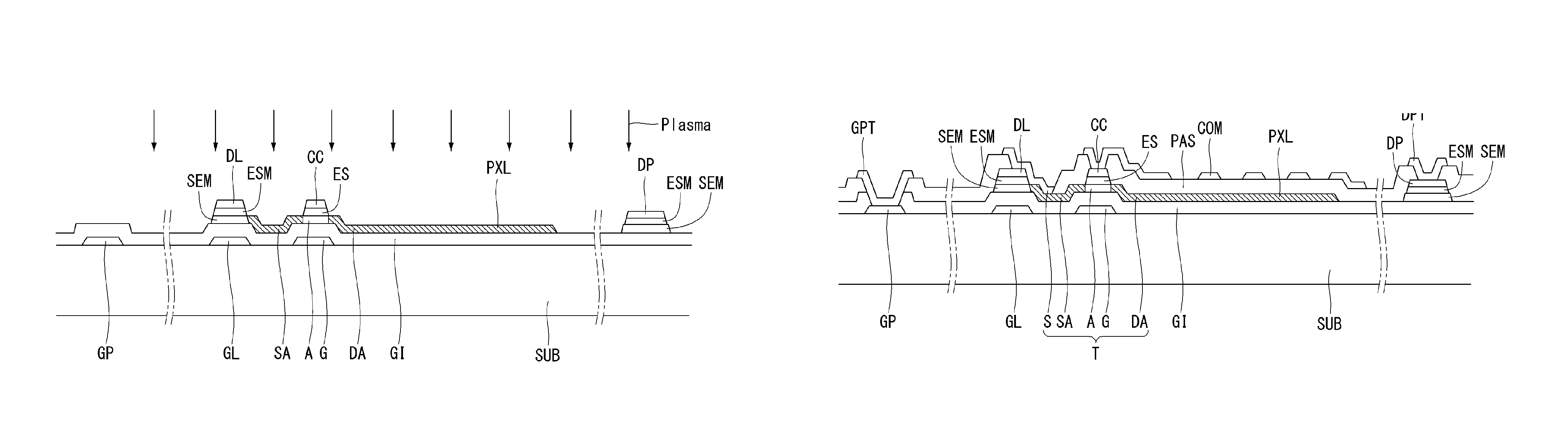
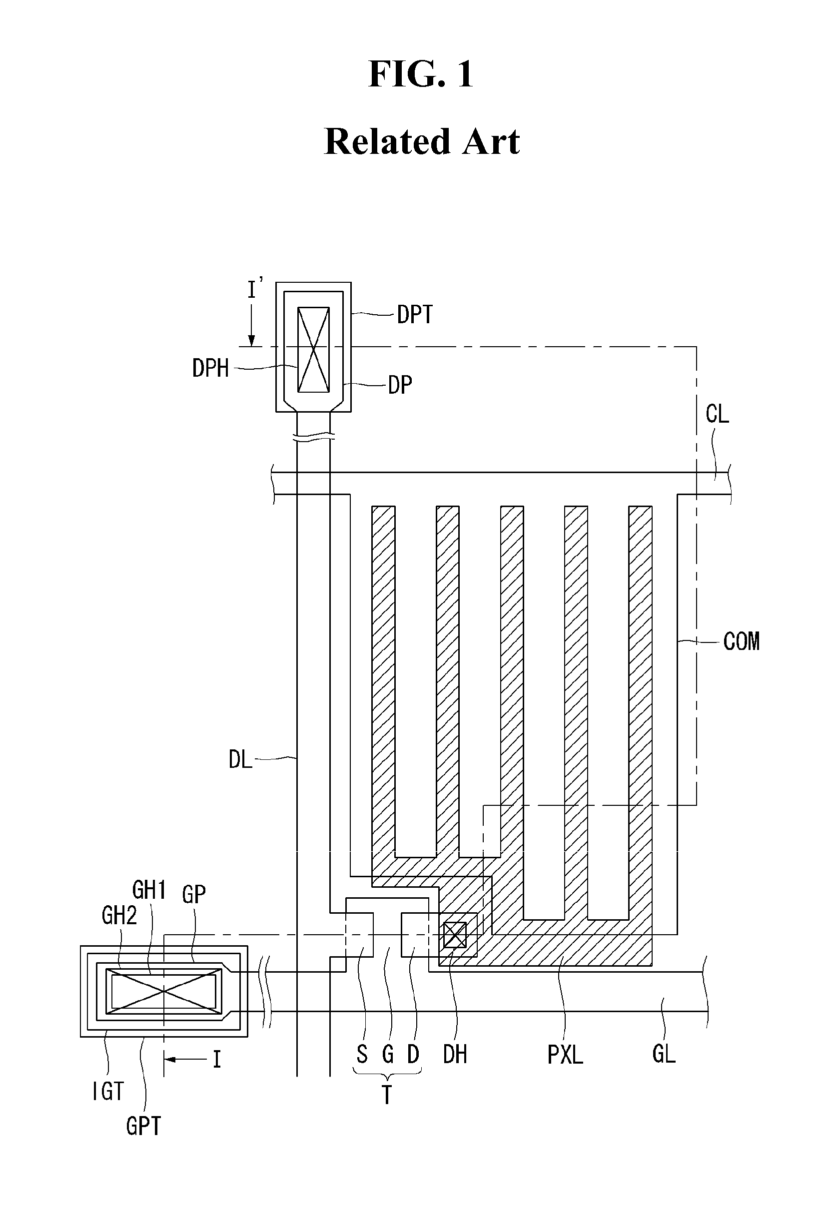
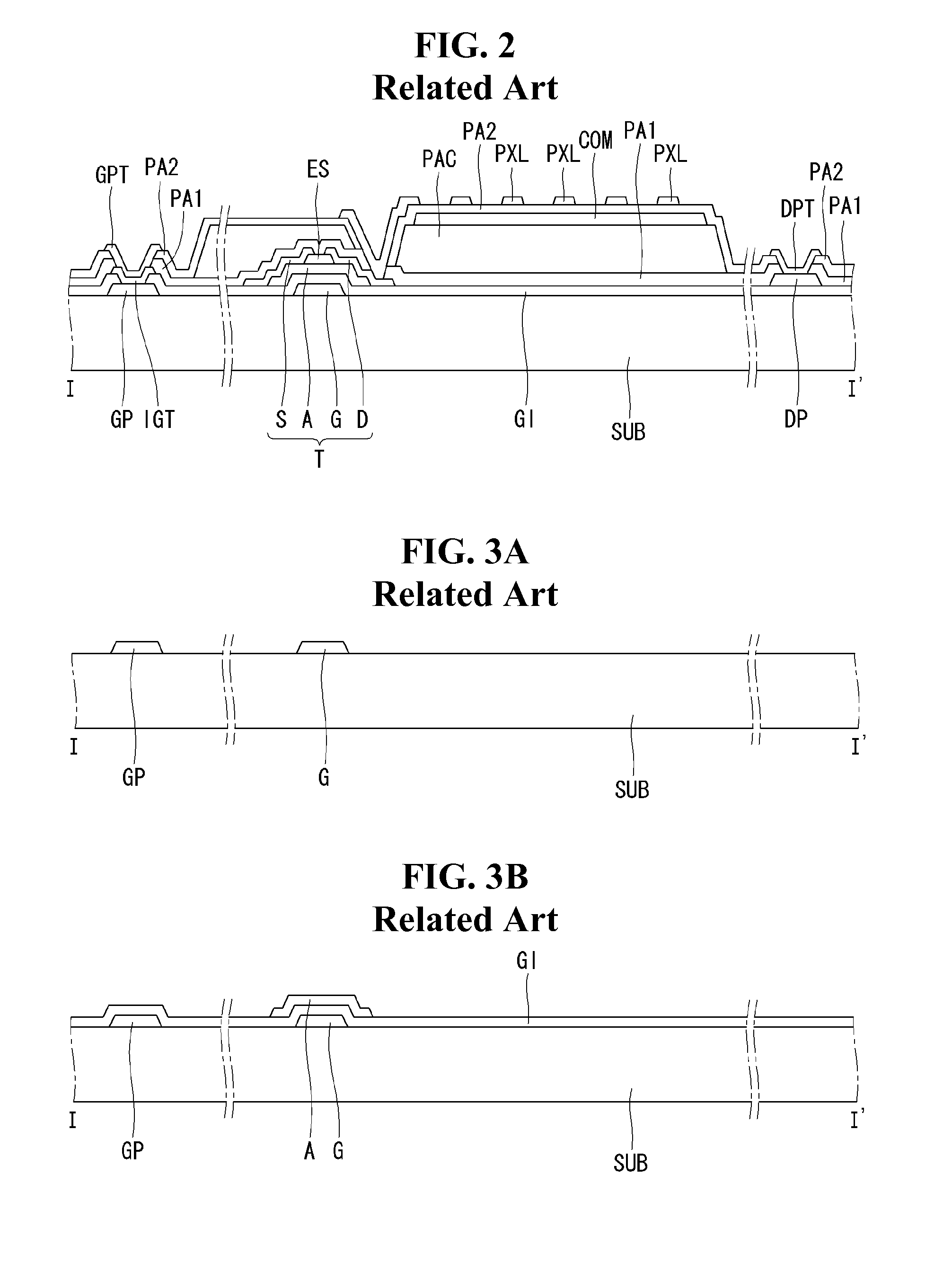
[0050]Referring to FIGS. 4 and 5A to 5D, we will explain about the preferred embodiment of the present disclosure. FIG. 4 is a plane view illustrating a thin film transistor substrate having an oxide semiconductor layer included in a fringe field type liquid crystal display according to the present disclosure. FIGS. 5A to 5D cross-sectional views along to the cutting line II-II′ in FIG. 4 for illustrating the manufacturing processes of the fringe field type thin film transistor according to the present disc...


PUM


Abstract

The present disclosure relates to a thin film transistor substrate having a metal oxide semiconductor for the fringe field type flat panel displays and a method for manufacturing the same. The thin film transistor substrate having an oxide semiconductor layer can include a substrate including pixel region; a gate element formed on the substrate; a gate insulating layer covering the gate element; a channel layer on the gate insulating layer, a source area expanded form a first side of the channel layer, a drain area expanded from a second side of the channel layer, and a pixel electrode expanded from the drain area to the pixel region; an etch stopper formed on the channel layer; a data element formed on the etch stopper; and a common electrode formed on the passivation layer and within the pixel region.

Description

CROSS-REFERENCE TO RELATED APPLICATION[0001]This application claims priority to Patent Application No. 10-2013-0073965 filed in Republic of Korea on Jun. 26, 2013, which is incorporated by reference herein in its entirety.BACKGROUND OF THE INVENTION[0002]1. Field of the Invention[0003]The present disclosure relates to a thin film transistor (or “TFT”) substrate having a metal oxide semiconductor for the fringe field type flat panel displays and a method for manufacturing the same. Especially, the present disclosure relates to a thin film transistor substrate for the flat panel display in which an oxide semiconductor material is used for an active layer, a source-drain electrode and a pixel electrode by simplifying the manufacturing mask process, and a manufacturing method the same.[0004]2. Discussion of the Related Art[0005]Nowadays, as the information society is developed, the requirements of displays for representing information are increasing. Accordingly, the various flat panel ...

Claims


Application Information

Patent Timeline
Patent Type & Authority Patents(United States)
IPC IPC(8): H01L27/12
CPCH01L27/1225H01L27/124H01L27/1288G02F1/134309G02F1/13439G02F1/13458G02F1/136286
Inventor JANG, HUNLEE, SUL
Owner LG DISPLAY CO LTD
Why Eureka
Try Eureka