Isotropic atomic layer etch for silicon and germanium oxides

a technology of germanium oxides and atomic layers, applied in the direction of coatings, chemical vapor deposition coatings, electric discharge tubes, etc., can solve the problems of high undesired native oxides and other oxides, limited control methods for one or several atomic layers removal, and high difficulty in further processing steps, etc., to achieve rapid and controlled temperature changes

Active Publication Date: 2016-08-30
LAM RES CORP
View PDF105 Cites 124 Cited by
  • Summary
  • Abstract
  • Description
  • Claims
  • Application Information

AI Technical Summary

Benefits of technology

[0019]In another aspect, an etching apparatus for controllably etching an oxide on a substrate is provided. The apparatus includes: a process chamber having an inlet for introduction of process gases; a substrate support in the process chamber configured for holding the substrate in position during etching of the oxide on the substrate; and a controller comprising program instructions for performing the steps of any of the methods described herein. For example the controller may include program instructions for: (a) contacting the substrate housed in the process chamber with an active hydrogen-containing species to modify the surface of the oxide on the substrate, wherein the active hydrogen-containing species is a compound containing one or more OH groups, or a hydrogen-containing species generated in a hydrogen containing plasma, and wherein the oxide is selected from the group consisting of silicon oxide, germanium oxide (including doped and undoped oxides) and combinations thereof; (b) removing non surface-bound active hydrogen species from the process chamber after the surface of oxide is modified; (c) flowing an anhydrous HF into the process chamber after (b), wherein the anhydrous HF reacts with the modified surface of oxide and wherein the reaction generates water; and (d) removing the water generated in (c) from the surface of the substrate. The apparatus, in some embodiments, is equipped with a temperature controller that allows for rapid and controlled changes in temperature at the substrate.

Problems solved by technology

While atomic layer deposition (ALD) and atomic-scale epitaxial growth techniques have been developed, the methods for controlled removal of one or several atomic layers are still limited.
Silicon oxide also is inadvertently formed on the layers of silicon when the partially fabricated wafer is exposed to air.
Native oxide film together with oxide residue produced during etching and / or ashing frequently presents a problem for further processing steps.
When formed in the bottom of a silicon landed via or contact hole, native oxide and other oxides are highly undesired, since they raise the overall electrical resistance of the via after it is filled with conductive materials.
The etch rate of the silicon oxide is nearly constant over time; as such, these types of processes are not well suited to accurately control the amount of a layer to be etched uniformly and precisely over all the exposed surface on the substrate.
These processes cannot be applied for removal of defined amounts of material on an atomic scale.

Method used


Image

  • Isotropic atomic layer etch for silicon and germanium oxides
  • Isotropic atomic layer etch for silicon and germanium oxides
  • Isotropic atomic layer etch for silicon and germanium oxides

Examples


example 1

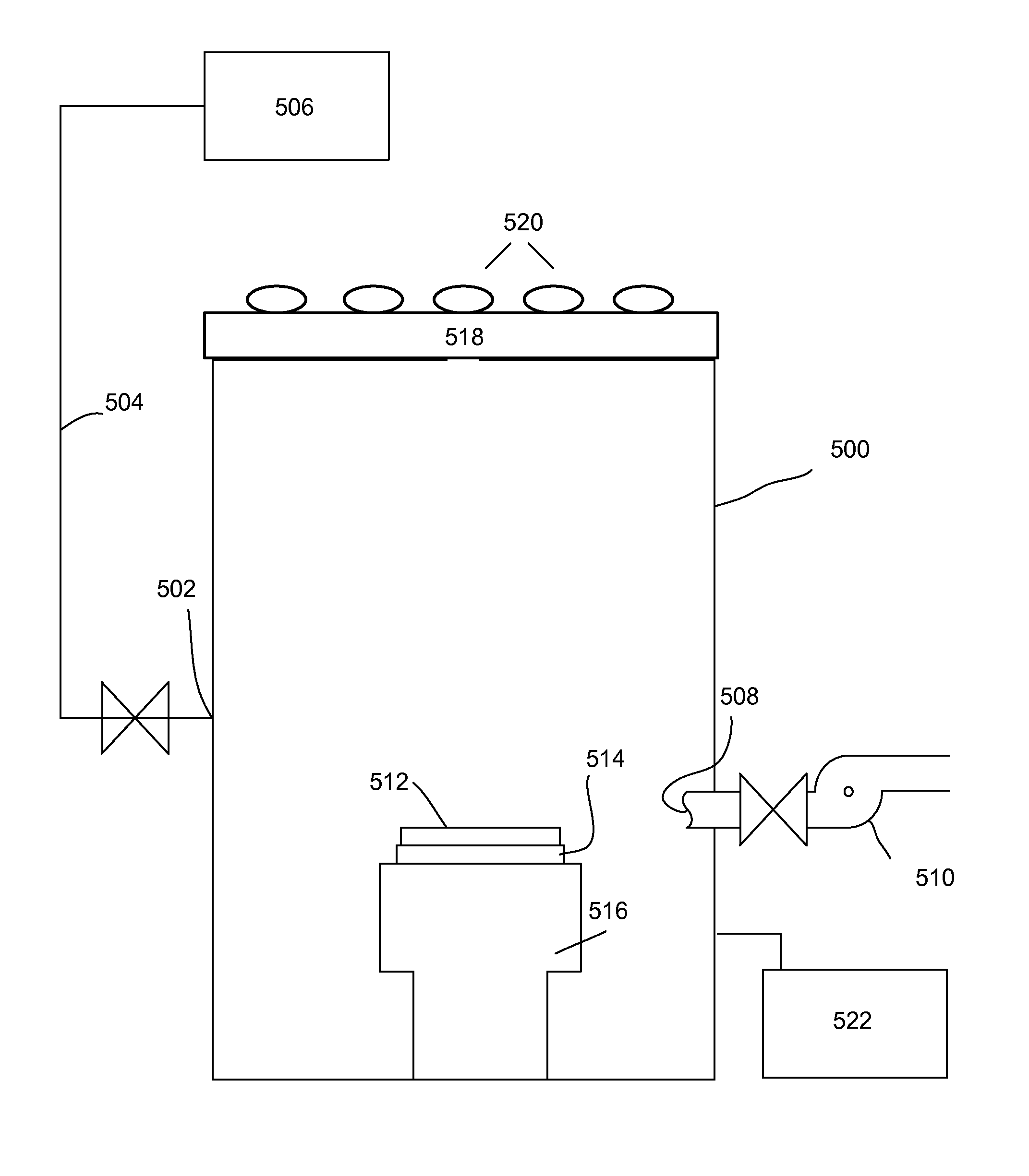
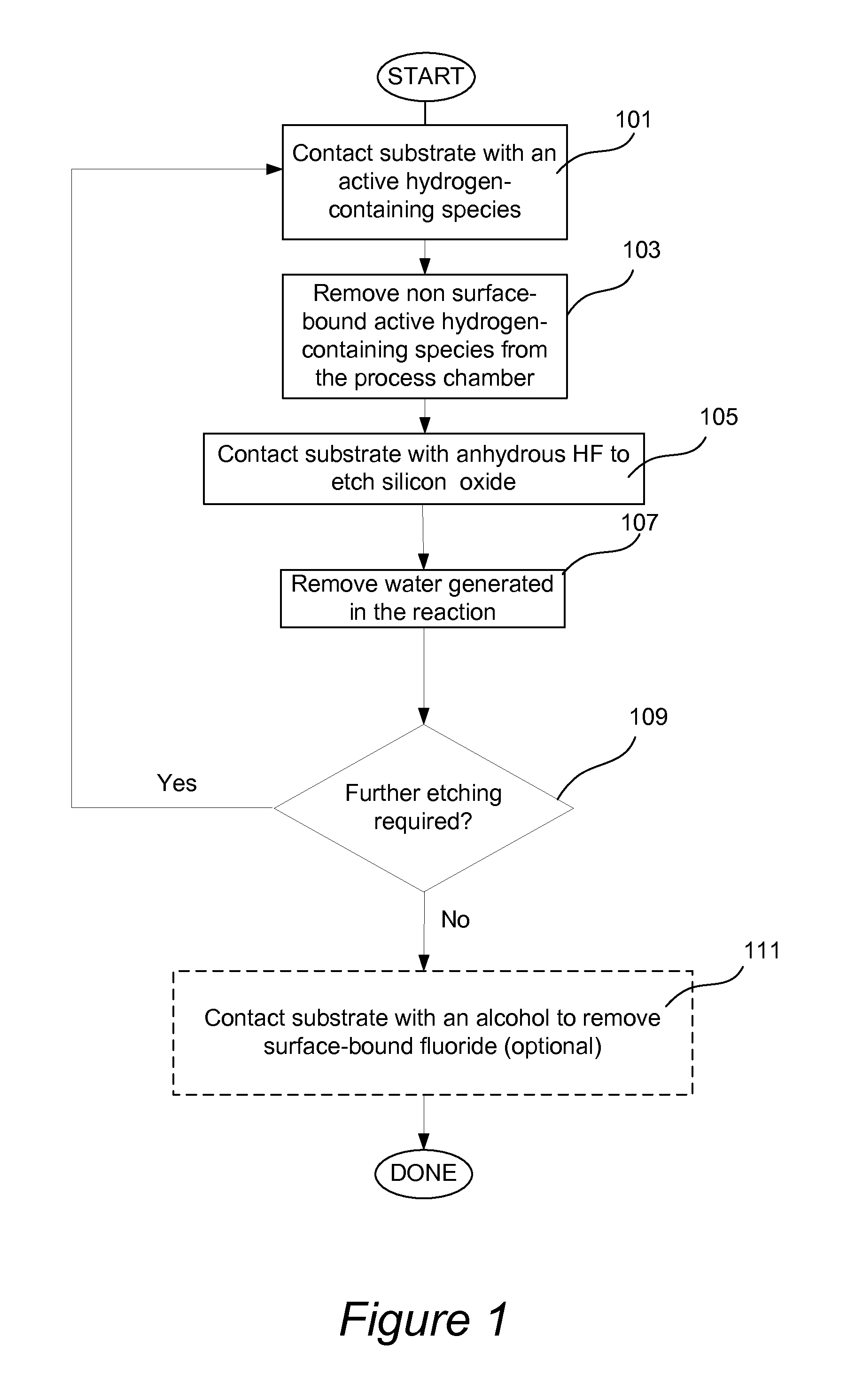
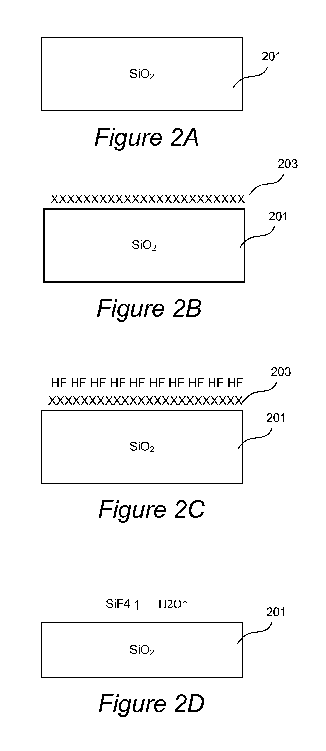
[0056]In this implementation, the entire etching cycle is performed at a sufficiently high temperature that does not allow water to stay adsorbed as it is generated in the etching reaction. In some embodiments, the etching process is performed at a temperature of at least about 80° C., such as between about 80° C.-300° C., e.g., between about 100° C.-300° C. The advantage of this method is that the temperature can be kept substantially constant during the entire etching cycle. Furthermore, because water is removed as it is generated during the etching reaction, the HF can be added in this embodiment in excess because the reaction will be limited by the amount of active hydrogen-containing species on the modified surface of the oxide after the first hydroxylation step. This embodiment, however, is not limited to using excess quantity of HF, and in some implementations, a controlled, limited amount of HF is dosed.

[0057]In one specific implementation of this example, the process makes ...

example 2

[0059]In this implementation water is removed from the surface of the substrate by electromagnetic irradiation (e.g., UV irradiation), by plasma treatment (e.g., by electrons, radicals and ions formed in a plasma) or by electron beam treatment. The water is removed from the substrate surface as it is generated in the reaction. The advantage of this implementation is that radiation-independent heating of the substrate is not necessary. Further, in this implementation, the choice of the active hydrogen-containing species that can modify the surface of oxide is more extensive than in Example 1. Similarly to Example 1, HF can be flowed in excess, because water is removed during the reaction, and the amount of removed oxide is determined by the amount of modified oxide in the first step. In this implementation the active hydrogen-containing species (water, an alcohol, a carboxylic acid, or a species generated in hydrogen plasma) contacts the substrate in period P1 and modifies the surfac...

example 3

[0060]In this embodiment water is removed from the surface of the substrate by raising the temperature to a temperature that is sufficient to desorb water and / or by lowering the pressure to achieve the conditions that desorb water from the substrate surface.

[0061]For example, the substrate may be treated with an active hydrogen-containing species at a first temperature. At some point after treatment with the active hydrogen-containing species, the temperature is raised to a second temperature that is sufficient to desorb water from the surface of the substrate. For example, if the active species is the species generated from a hydrogen-containing plasma, or if the active species is an alcohol or a carboxylic acid that has a vapor pressure that is lower or that is not significantly higher than the vapor pressure of water and the second temperature does not cause dehydroxylation of the surface of the substrate, the temperature may be raised as early as immediately after treatment with...


PUM

PropertyMeasurementUnit
temperatureaaaaaaaaaa
pressureaaaaaaaaaa

Abstract

Methods for controlled isotropic etching of layers of silicon oxide and germanium oxide with atomic scale fidelity are provided. The methods make use of a reaction of anhydrous HF with an activated surface of an oxide, with an emphasis on removal of water generated in the reaction. In certain embodiments the oxide surface is first modified by adsorbing an OH-containing species (e.g., an alcohol) or by forming OH bonds using a hydrogen-containing plasma. The activated oxide is then etched by a separately introduced anhydrous HF, while the water generated in the reaction is removed from the surface of the substrate as the reaction proceeds, or at any time during or after the reaction. These methods may be used in interconnect pre-clean applications, gate dielectric processing, manufacturing of memory devices, or any other applications where accurate removal of one or multiple atomic layers of material is desired.

Description

FIELD OF THE INVENTION[0001]The present invention pertains to methods of removing layers of material on a substrate. The methods are particularly useful for accurate isotropic removal of silicon dioxide and germanium dioxide with atomic scale fidelity on a semiconductor substrate.BACKGROUND OF THE INVENTION[0002]Fabrication of integrated circuit (IC) devices at a modern level of miniaturization demands techniques that can operate at an atomic scale. Certain components of IC devices now have dimensions of tens of Angstroms, corresponding to only a few atomic layers of material. For example, gate dielectric in modern IC transistors can have a thickness of only 12 Å, corresponding to only four atomic layers of silicon dioxide. It is often desirable to fine-tune the electronic properties of these components by altering their dimensions, which would involve deposition or removal of only a few atomic layers of material. While atomic layer deposition (ALD) and atomic-scale epitaxial growth...

Claims


Application Information

Patent Timeline
Patent Type & Authority Patents(United States)
IPC IPC(8): H01L21/302H01L21/311H01J37/32C23C16/458C23C16/50C23C16/52
CPCC23C16/458C23C16/50C23C16/52H01J37/32009H01J37/32449H01J37/32715H01L21/31116H01L21/0234H01L21/02343H01L21/67075
Inventor LILL, THORSTENBERRY, III, IVAN L.SHEN, MEIHUASCHOEPP, ALAN M.HEMKER, DAVID J.
Owner LAM RES CORP
Why Eureka
Try Eureka