Wiring board and high frequency module using same

a technology of high frequency module and wiring board, which is applied in the direction of high frequency circuit adaptation, waveguide, waveguide type device, etc., can solve the problems of high-frequency transmission loss, high-frequency transmission loss, dielectric loss of solder resist, etc., and achieve high frequency characteristics, high frequency module strength, and high frequency characteristics

Inactive Publication Date: 2016-08-30
PANASONIC CORP
View PDF11 Cites 0 Cited by
  • Summary
  • Abstract
  • Description
  • Claims
  • Application Information

AI Technical Summary

Benefits of technology

[0022]According to the disclosure, it is possible to provide a high frequency module wiring board in which the strength of each wiring is high while high frequency characteristics are kept without entirely removing a solder resist layer.

Problems solved by technology

On the other hand, when the solder resist serving as a dielectric substance is disposed near a wiring section in a board mounted with a high frequency circuit element (high frequency circuit chip) and a board for a high frequency antenna module, dielectric loss of the solder resist leads to high-frequency transmission loss.
However, dielectric loss of the solder resist layer 5 leads to high-frequency transmission loss.

Method used


Image

  • Wiring board and high frequency module using same
  • Wiring board and high frequency module using same
  • Wiring board and high frequency module using same

Examples


embodiment 1

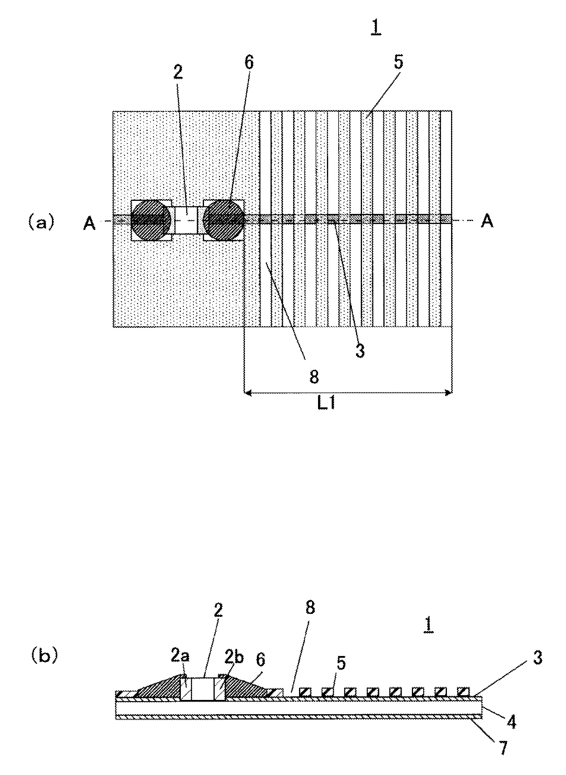
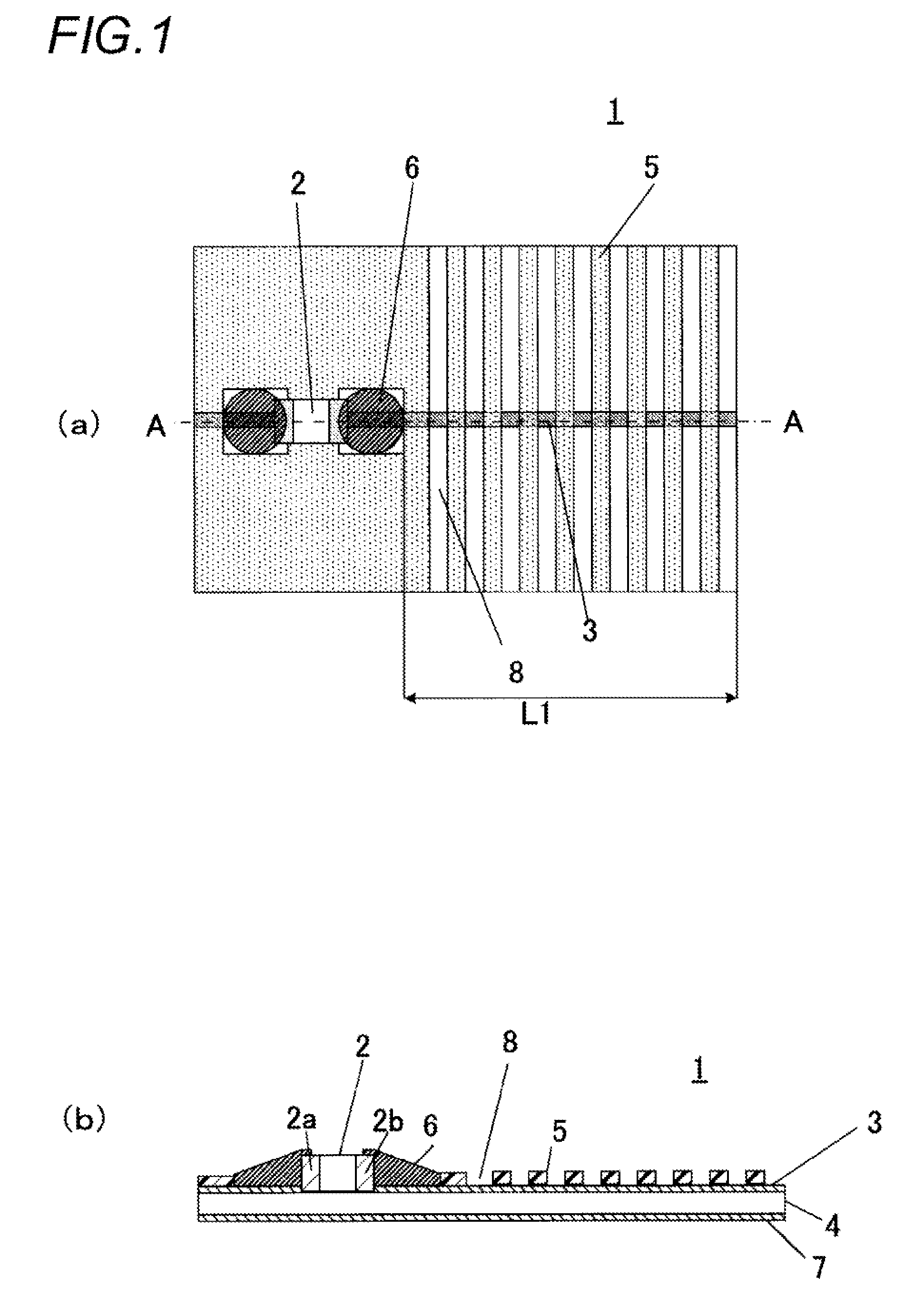
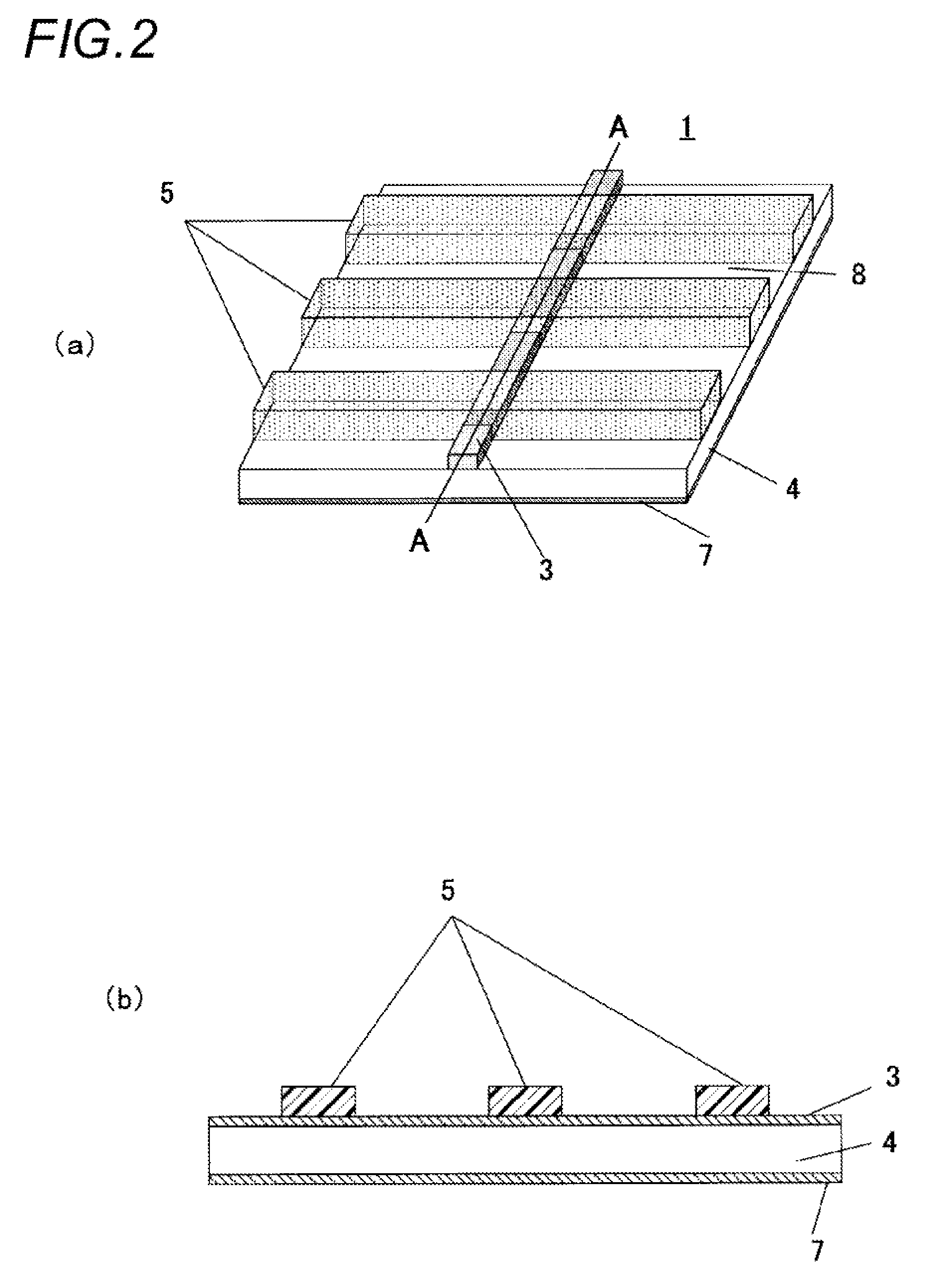
[0065]FIG. 1(a) is an explanatory view (top view) showing a main portion configuration of a high frequency module using a high frequency module wiring board according to Embodiment 1 of the disclosure, and FIG. 1(b) is an explanatory view (sectional view) cut in a wiring direction. FIG. 2(a) is a main portion perspective view of a wiring section, and FIG. 2(b) is a sectional view taken on the line A-A in FIG. 2(a). FIG. 3 is an overall schematic view of the high frequency module.

[0066]FIG. 4 is a top view showing a pattern of a solder resist layer near a surface mount type chip component (SMT component) 2. FIG. 5 is a top view showing the pattern of the solder resist layer near a high frequency IC chip 9 which is an SMT component with a three-terminal structure.

[0067]A wiring board 1 for a high frequency module according to the embodiment includes wiring sections 3 for high frequency transmission, and a solder resist layer 5 formed on the wiring sections 3. Openings 8 of the solder ...

embodiment 2

[0092]FIG. 9 is a view showing a main portion configuration of a high frequency module using a high frequency module wiring board according to Embodiment 2 of the disclosure. FIG. 9 is a top view showing a pattern of a solder resist layer 5 near a surface mount type chip component (SMT component) 2.

[0093]The solder resist layer in Embodiment 2 has circular openings 8c provided at predetermined intervals in the pattern of the solder resist layer 5 on the wiring section 3. The other portions, for example, the configuration of the wiring section are similar to those in the embodiment, and description thereof will be omitted here.

[0094]Incidentally, in the same manner as in Embodiment 1, it is desirable that the intervals of the openings 8c are set at about λg / 8 or less.

[0095]In addition, the portions to which a solder resist is not applied, that is, the openings are not limited to stripe-like openings, quadrangular openings or circular openings, but they may be formed as polygonal open...

embodiment 3

[0097]FIG. 11(a) and FIG. 11(b) are views showing a main portion configuration of a high frequency module using a high frequency module wiring board according to Embodiment 3 of the disclosure. FIG. 11(a) is a top view showing the main portion configuration of the high frequency module using the high frequency module wiring board according to Embodiment 3 of the disclosure, and FIG. 11(b) is a sectional view (sectional view taken on the line A-A) cut in a wiring direction.

[0098]In the same manner as in Embodiment 1, openings 8 shaped like stripes are formed in a solder resist layer in the high frequency module wiring board in Embodiment 3. However, the solder resist layer 5 on each wiring section 3 is left as it is, while the solder resist layer 5 on opposite sides of the wiring section 3 is removed. Thus, side openings 8s are formed on the opposite sides of the wiring section 3.

[0099]Incidentally, the other portions including the configuration of the wiring section 3 are similar to...


PUM


Abstract

A high frequency module wiring board includes a wiring section for high frequency transmission, and a solder resist layer formed upon the wiring section. The solder resist layer covers the wiring section so as to have an opening section at a part of the wiring section in a region extending within a predetermined distance from an input / output terminal of a chip component.

Description

TECHNICAL FIELD[0001]The present disclosure relates to a wiring board and a high frequency (microwave or millimeter wave) module using the same. Particularly, it relates to a high frequency module in which a high frequency circuit chip such as a wireless IC is mounted on a wiring board.BACKGROUND ART[0002]There has been widely used a technique in which a dielectric substance called a solder resist is applied to a portion which is not soldered in a board mounted with an SMT (Surface Mount Technology) component so that solder is restricted from extending over the board.[0003]On the other hand, when the solder resist serving as a dielectric substance is disposed near a wiring section in a board mounted with a high frequency circuit element (high frequency circuit chip) and a board for a high frequency antenna module, dielectric loss of the solder resist leads to high-frequency transmission loss. An example of a wiring board covered with a solder resist layer is shown in FIG. 41(a) and ...

Claims


Application Information

Patent Timeline
Patent Type & Authority Patents(United States)
IPC IPC(8): H01L23/66H01L21/56H05K3/34H01P3/08H01P3/16H05K1/02H01P5/02H01L25/16H01L23/00
CPCH01L21/563H01L23/66H05K3/3452H01P3/081H01P3/16H01L2224/16225H01L2224/32225H01L2224/48091H01L2224/48227H01L2224/73204H01L2924/00014H01L2224/73265H01L2924/00012H05K1/024H05K1/0243H01L2924/1423H01L2924/3011H01L2924/00H01P5/028H01L25/16H01L2223/6627H01L24/73
Inventor SHIOZAKI, RYOSUKEFUJITA, SUGURU
Owner PANASONIC CORP
Why Eureka
Try Eureka