Organic light-emitting device emitting delayed fluorescence

a light-emitting device and organic technology, applied in the direction of organic semiconductor devices, solid-state devices, semiconductor devices, etc., can solve the problems of reducing the charge transport characteristics, and achieve the effect of improving the roll-off characteristics, reducing the efficiency roll-off characteristics, and high efficiency

Active Publication Date: 2016-08-30
SAMSUNG DISPLAY CO LTD
View PDF15 Cites 3 Cited by
  • Summary
  • Abstract
  • Description
  • Claims
  • Application Information

AI Technical Summary

Benefits of technology

[0010]One or more aspects of one or more embodiments of the present disclosure relate to an organic light-emitting device including an emission layer emitting blue delayed fluorescence with high efficiency and improved roll-off characteristics (e.g., decreased efficiency roll-off characteristics).

Problems solved by technology

For example, when the host has a high triplet energy level, charges may not be effectively injected from adjacent layers due to the host's large band gap energy, and because of the host's short conjugation length, charge transport characteristics may decrease.

Method used


Image

  • Organic light-emitting device emitting delayed fluorescence
  • Organic light-emitting device emitting delayed fluorescence
  • Organic light-emitting device emitting delayed fluorescence

Examples


example 1

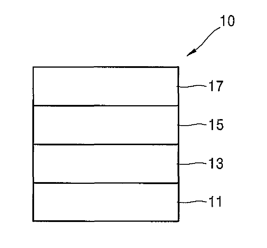
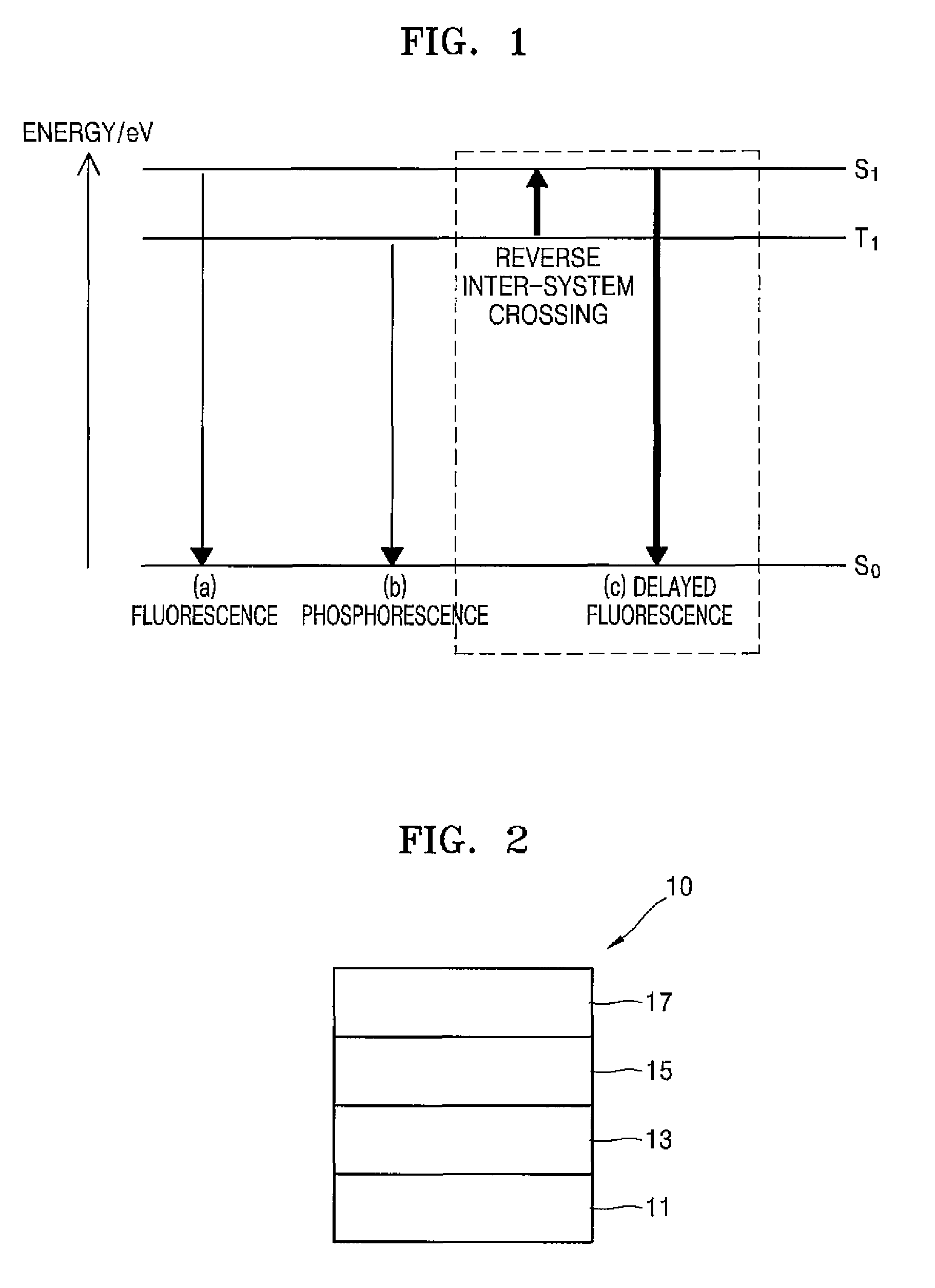
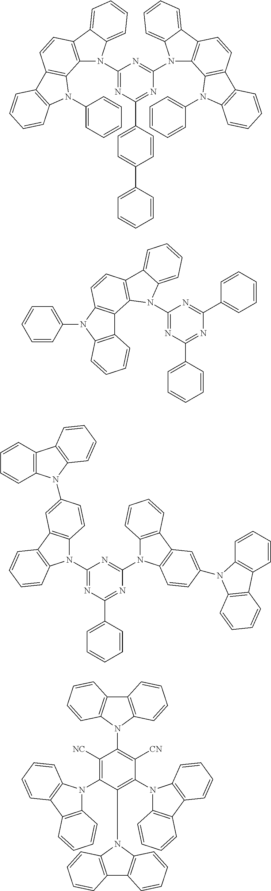
[0181]As an anode, an ITO glass substrate having a thickness of 15 Ω / cm2 (1200 Å) and made by Corning Inc. was cut to a size of 50 mm×50 mm×0.5 mm and then, sonicated in acetone, in isopropyl alcohol, and in pure water, for 15 minutes in each, and then, cleaned using UV ozone for 30 minutes. Next, methylated-NPD was vacuum deposited on an upper portion of the ITO glass substrate to form a hole injection layer having a thickness of 600 Å and then, TAPC was vacuum deposited on an upper portion of the hole injection layer to form a hole transport layer having a thickness of 300 Å. Compound H5 and Compound H1 were used as a host in a weight ratio of 90:10 (Compound H5:Compound H1), and the resulting host and a blue emitting dopant, which was Compound D1, were co-deposited on an upper portion of the hole transport layer in a weight ratio of 94:6 (host:dopant) to form an emission layer having a thickness of 300 Å. TPBi was vacuum deposited on an upper portion of the emission layer to form...

example 2

[0182]An organic light-emitting device was manufactured in the same (or substantially the same) manner as in Example 1, except that Compound H6 and Compound H3 were used as a host of an emission layer in a weight ratio of 90:10 (Compound H6:Compound H3) instead of Compound H5 and Compound H1 in a weight ratio of 90:10.

example 3

[0183]An organic light-emitting device was manufactured in the same (or substantially the same) manner as in Example 1, except that Compound H6 and Compound H7 were used as a host of an emission layer in a weight ratio of 90:10 (Compound H6:Compound H7) instead of Compound H5 and Compound H1 in a weight ratio of 90:10.


PUM


Abstract

An organic light-emitting device includes a first electrode; a second electrode facing the first electrode; and an emission layer between the first electrode and the second electrode, the emission layer including a dopant, a first host, and a second host. The dopant is a delayed fluorescence emitting material, and a triplet energy of the first host, EH1(T1) and a triplet energy of the second host, EH2(T1) are each equal to or greater than a triplet energy of the dopant, ED(T1). The triplet energy of the first host, EH1(T1) is in a range of about 2.6 eV to about 3.1 eV.

Description

CROSS-REFERENCE TO RELATED APPLICATION[0001]This application claims priority to and the benefit of Korean Patent Application No. 10-2014-0125245, filed on Sep. 19, 2014, in the Korean Intellectual Property Office, the entire disclosure of which is incorporated herein by reference.BACKGROUND[0002]1. Field[0003]One or more aspects of one or more embodiments of the present disclosure relate to an organic light-emitting device emitting delayed fluorescence.[0004]2. Description of the Related Art[0005]In an organic light-emitting device (OLED), holes provided from an anode and electrons provided from a cathode are combined in an organic emission layer formed between the anode and the cathode to generate light. Such OLED devices typically have good color reproduction properties and color purity, short response times, self-emitting characteristics, small thickness, light-weight properties, high contrast ratios, side viewing angles, low driving voltages, and / or low power consumptions. Due t...

Claims


Application Information

Patent Timeline
Patent Type & Authority Patents(United States)
IPC IPC(8): H01L51/00H01L51/52H01L51/50
CPCH01L51/0058H01L51/0072H01L51/5012H01L2251/5384H01L2251/308H01L2251/301H01L51/5206H01L51/5221H01L51/5016H01L51/5056H01L51/5072H01L51/5096H01L51/5088H01L51/5092H01L51/006H01L51/0067H01L2251/552H10K85/633H10K85/654H10K85/6572H10K50/11H10K2101/90H10K2101/30H10K85/626H10K50/15H10K50/16H10K50/17H10K50/18H10K50/81H10K50/82H10K50/171H10K2101/10H10K2102/00H10K2102/103
Inventor KIM, YOUNSUNKIM, SEULONGSHIN, DONGWOOLEE, JUNGSUBITO, NAOYUKI
Owner SAMSUNG DISPLAY CO LTD
Why Eureka
Try Eureka