Method for producing multi-layer substrate and multi-layer substrate
a technology of multi-layer substrates and substrates, applied in the direction of printed circuit non-printed electric components, semiconductor/solid-state device details, non-metallic protective coating applications, etc., can solve the problems of reducing the reliability with which a multi-layer substrate is mounted, and disconnection of a conductor provided on the multi-layer substra
- Summary
- Abstract
- Description
- Claims
- Application Information
AI Technical Summary
Benefits of technology
Problems solved by technology
Method used
Image

Examples
first embodiment
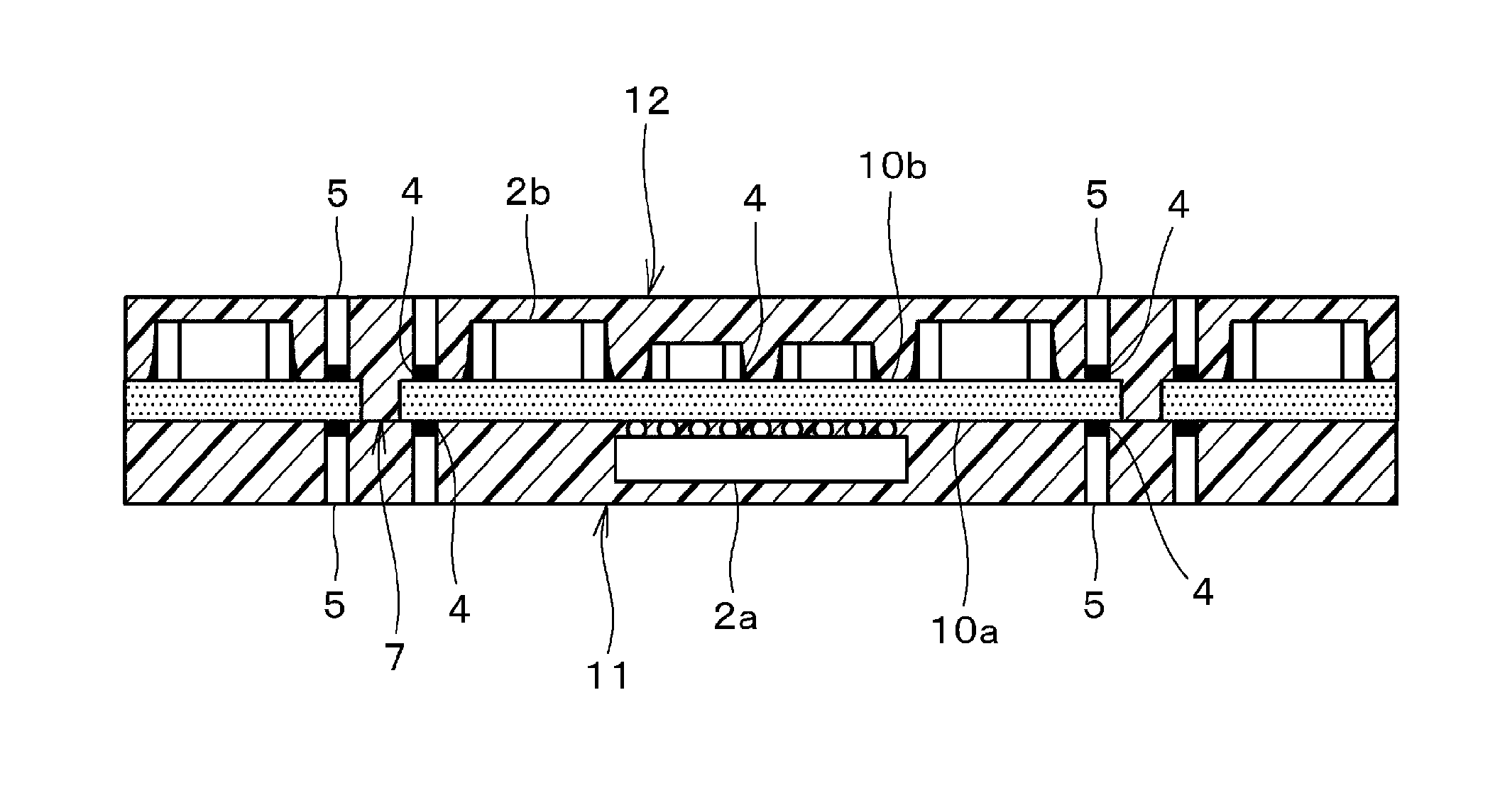
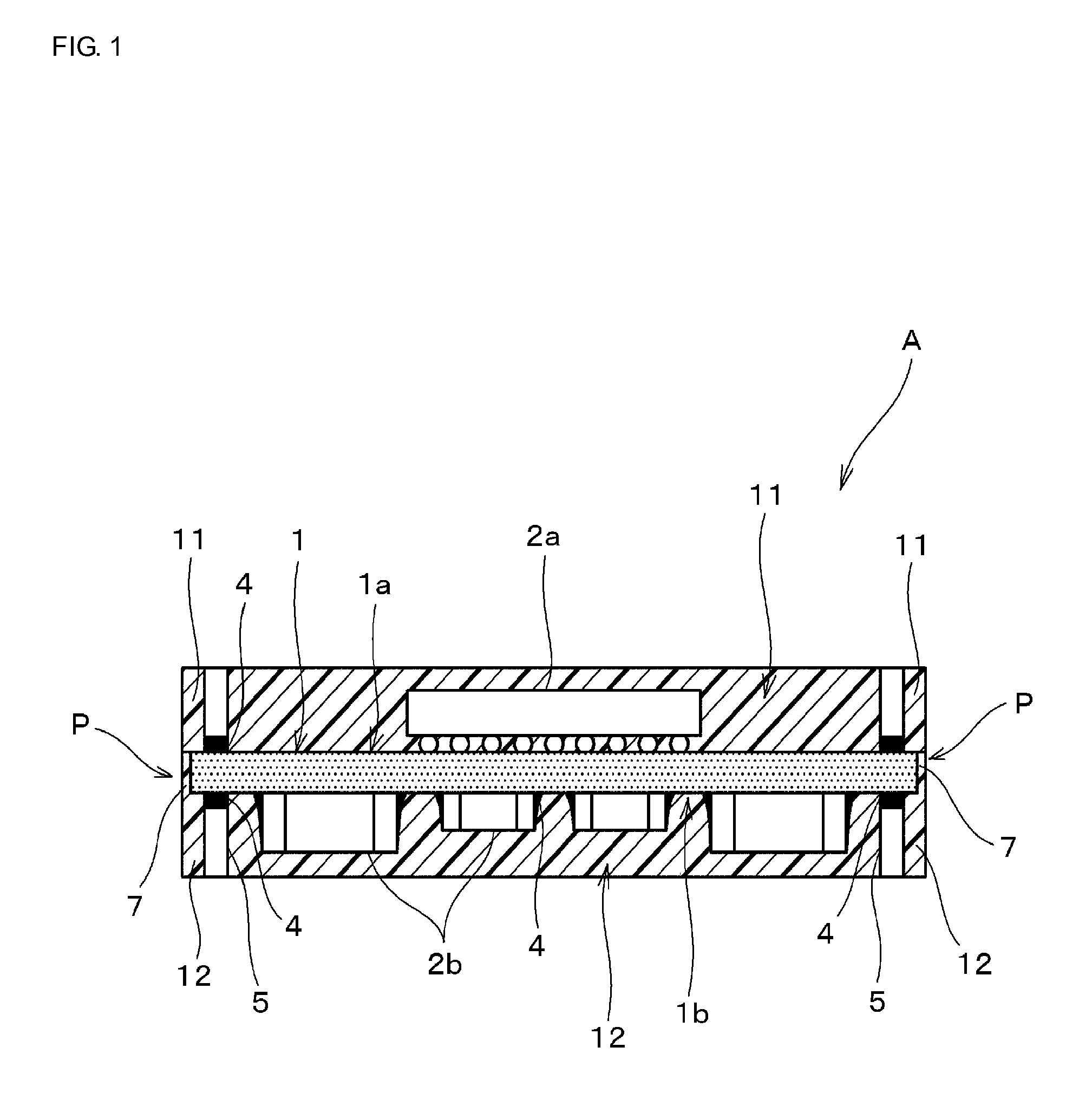
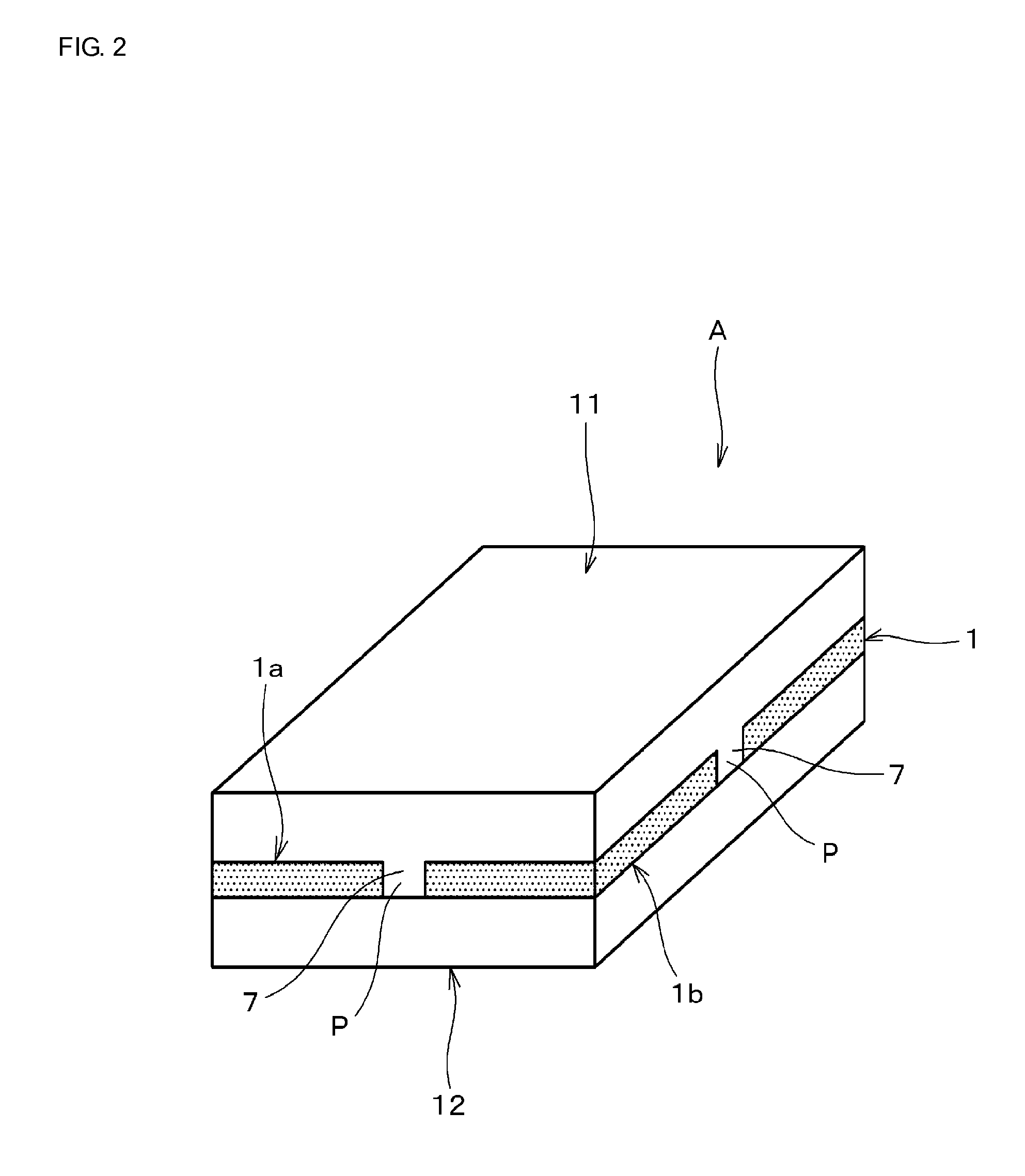
[0047]FIG. 1 is a front sectional view of a structure of a multi-layer substrate according to an embodiment (first embodiment) of the present invention. FIG. 2 is a perspective view thereof. FIG. 3 is a plan sectional view illustrating a mode of arrangement of regions where resin layers are joined in the multi-layer substrate according to the first embodiment of the present invention.
[0048]As shown in FIGS. 1 and 2, a multi-layer substrate A according to the first embodiment includes a core individual substrate 1, a surface mount device (for example, an active chip component such as a semiconductor device) 2a, a surface mount device (for example, a passive chip component such as a capacitor) 2b, straight terminals 5, both principal surfaces 1a and 1b of the core individual substrate 1, and resin layers 11 and 12. The surface mount device 2a is mounted on the principal surface 1a of the core individual substrate by flip-chip mounting. The surface mount device 2b is mounted on the pri...
second embodiment
[0088]FIGS. 13(a) and 13(b) show a multi-layer substrate B according to another embodiment (second embodiment) of the present invention. For facilitating understanding, FIGS. 13(a) and 13(b) only show a core individual substrate 1 and resin layers 11 and 12, with the other structural features not being shown.
[0089]As shown in FIGS. 13(a) and 13(b), in the multi-layer substrate B according to the second embodiment, the resin layers 11 and 12, formed on both principal surfaces of the core individual substrate 1, are integrally joined to each other via a through hole 17 that extends through the core individual substrate 1.
[0090]Even the structure according to the second embodiment can provide effects that are similar to those provided by the first embodiment.
[0091]The multi-layer substrate B according to the second embodiment may be produced by a method that is in accordance with the producing method according to the first embodiment. That is, when forming through holes in the core par...
PUM
| Property | Measurement | Unit |
|---|---|---|
| Thermal stress | aaaaa | aaaaa |
| stress | aaaaa | aaaaa |
| structure | aaaaa | aaaaa |
Abstract
Description
Claims
Application Information
 - R&D
- Intellectual Property
- Life Sciences
- Materials
- Tech Scout
- Unparalleled Data Quality
- Higher Quality Content
- 60% Fewer Hallucinations
Browse by: Latest US Patents, China's latest patents, Technical Efficacy Thesaurus, Application Domain, Technology Topic, Popular Technical Reports.
© 2025 PatSnap. All rights reserved.Legal|Privacy policy|Modern Slavery Act Transparency Statement|Sitemap|About US| Contact US: help@patsnap.com