Semiconductor device and production method therefor

a production method and semiconductor technology, applied in the direction of semiconductor devices, basic electric elements, electrical appliances, etc., can solve the problems of deterioration of the bonding strength, unilluminable light emitting diodes and the like, and the resin itself that is used in resin bonding to deteriorate, and achieve the effect of simple production method and high heat releasability

Active Publication Date: 2010-07-29
NICHIA CORP
View PDF14 Cites 25 Cited by
  • Summary
  • Abstract
  • Description
  • Claims
  • Application Information

AI Technical Summary

Benefits of technology

[0021]By adopting the above-described configuration, a low-cost reliable semiconductor device that does not include components that undergo deterioration and a production method therefor can be provided. Moreover, sin

Problems solved by technology

However, the heat generation due to the recent increase of light energy attained by light emitting diodes, laser diodes and like devices as well as the recent increase in input electricity; causes the resin itself that is used in resin bonding to deteriorate with time, resulting in problems such as discoloration and deterioration of the bonding strength.
Moreover, resin bonding that uses only an epoxy resin and resin bonding that uses a silver paste both have a problem in that, since they have poor thermal conductivity and insufficient heat releasability,

Method used


Image

  • Semiconductor device and production method therefor
  • Semiconductor device and production method therefor

Examples


first embodiment

Semiconductor Device of the First Embodiment

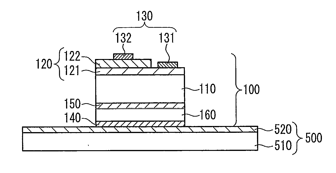
[0042]An example of the semiconductor device of the first embodiment is described with reference to a drawing. FIG. 1 is a schematic cross-sectional drawing showing the semiconductor light emitting element of the first embodiment when mounted. A description is given with reference to a light emitting semiconductor element that uses a light emitting diode as a semiconductor element, but the present invention is applicable also to transistors, ICs, LSIs, and the like other than light emitting semiconductor elements.

[0043]In the semiconductor device, silver or silver oxide 520 provided on a surface of a base 500 and silver or silver oxide 140 provided on a surface of a light emitting semiconductor element 100 are directly bonded.

[0044]The light emitting semiconductor element 100 includes a translucent inorganic substrate 110, a semiconductor layer 120 that emits light, an electrode 130 disposed on the semiconductor layer 120, first silver 150...

second embodiment

Semiconductor Device of the Second Embodiment

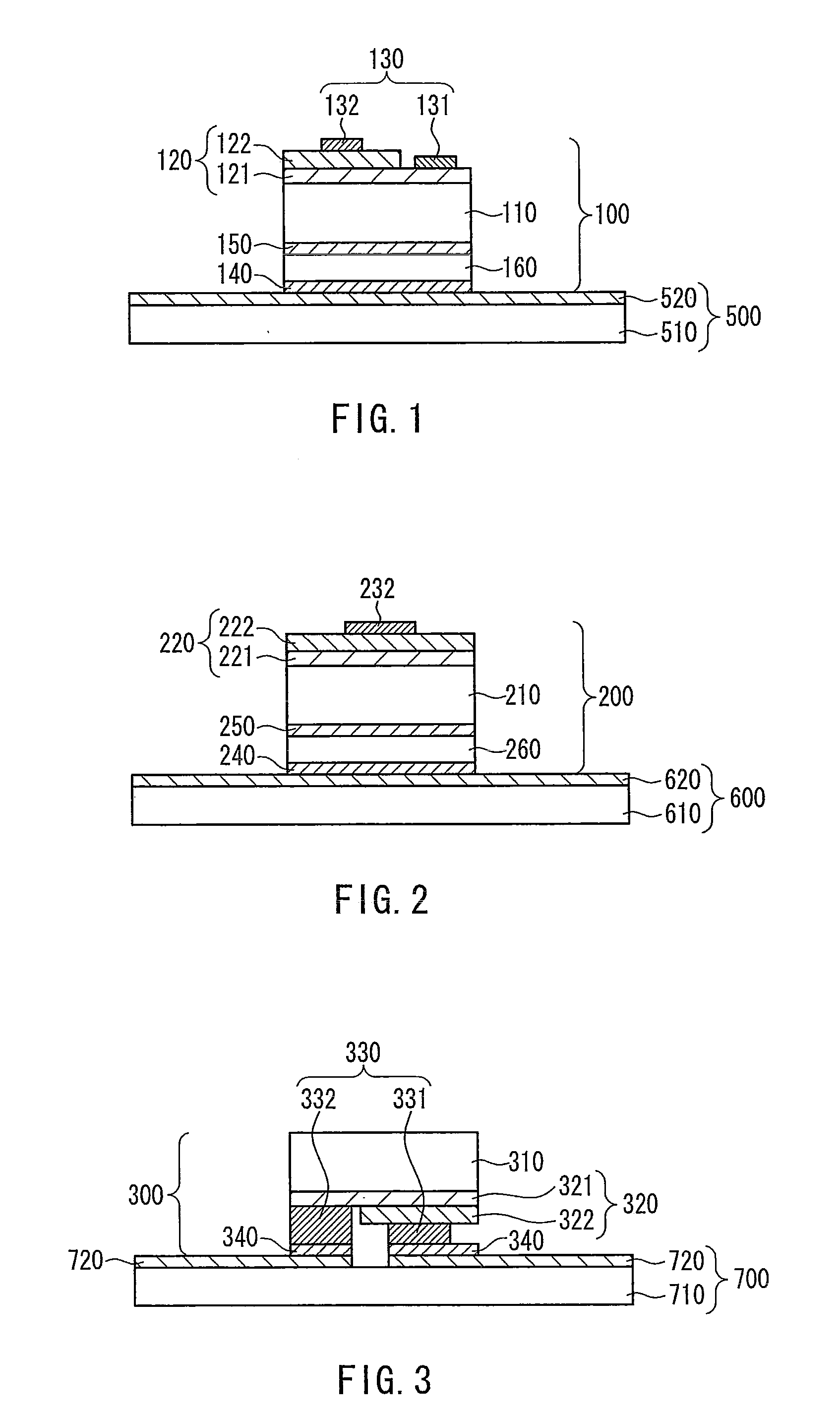
[0057]An example of the semiconductor device of the second embodiment is described with reference to a drawing. FIG. 2 is a schematic cross-sectional drawing showing the semiconductor light emitting element of the second embodiment when mounted. The semiconductor device of the second embodiment has substantially the same configuration as the semiconductor device of the first embodiment except for the light emitting semiconductor element, and some descriptions may be omitted.

[0058]In the semiconductor device, silver or silver oxide 620 provided on a surface of a base 600 and silver or silver oxide 240 provided on a surface of a light emitting semiconductor element 200 are bonded.

[0059]The light emitting semiconductor element 200 includes a translucent inorganic substrate 210, a semiconductor layer 220 that emits light, a p-type electrode 232 disposed on the semiconductor layer 220, first silver 250 provided on the side opposite the side on...

third embodiment

Semiconductor Device of the Third Embodiment

[0062]An example of the semiconductor device of the third embodiment is described with reference to a drawing. FIG. 3 is a schematic cross-sectional drawing showing the semiconductor light emitting element of the third embodiment when mounted. The semiconductor device of the second embodiment have substantially the same configuration as the semiconductor device of the first embodiment except for the light emitting semiconductor element, and some descriptions may be omitted.

[0063]In the semiconductor device, silver or silver oxide 720 provided on a surface of a base 700 and silver or silver oxide 340 provided on a surface of a light emitting semiconductor element 300 are bonded.

[0064]The light emitting semiconductor element 300 includes a translucent inorganic substrate 310, a semiconductor layer 320 that emits light, an electrode 330 disposed on the semiconductor layer 320, and silver or silver oxide 340 provided on the electrode 330. In t...


PUM


Abstract

An object of the invention is to provide a method for producing a conductive member having low electrical resistance, and the conductive member is obtained using a low-cost stable conductive material composition that does not contain an adhesive. A method for producing a semiconductor device in which silver or silver oxide provided on a surface of a base and silver or silver oxide provided on a surface of a semiconductor element are bonded, includes the steps of arranging a semiconductor element on a base such that silver or silver oxide provided on a surface of the semiconductor element is in contact with silver or silver oxide provided on a surface of the base, and bonding the semiconductor element and the base by applying heat having a temperature of 200 to 900° C. to the semiconductor device and the base.

Description

BACKGROUND OF THE INVENTION[0001]1. Field of the Invention[0002]The present invention relates to a semiconductor device and a production method therefor, especially, a method for bonding a semiconductor element (hereinafter sometimes referred to as a “die-attach method”).[0003]2. Description of Related Art[0004]Various bonding methods for mounting semiconductor elements such as transistors, ICs, and LSIs have been known. In addition, various bonding methods that are suitable with, among semiconductor elements, light emitting semiconductor elements such as light emitting diodes (hereinafter sometimes referred to as “LEDs”) and laser diodes (hereinafter sometimes referred to as “LDs”) have been know as well.[0005]Conventionally, die-attach methods for semiconductor elements are roughly classified into two categories, i.e., bonding methods that use epoxy resin adhesives (hereinafter referred to as “resin bonding”) and bonding methods that use eutectic metals having an eutectic point at...

Claims


Application Information

Patent Timeline
IPC IPC(8): H01L21/60
CPCH01L21/187H01L24/17H01L24/29H01L24/32H01L24/81H01L24/83H01L33/62H01L2224/13099H01L2224/16225H01L2224/16227H01L2224/812H01L2224/81801H01L2224/81894H01L2224/83801H01L2224/8383H01L2924/01004H01L2924/01012H01L2924/01013H01L2924/0102H01L2924/01022H01L2924/01025H01L2924/01029H01L2924/0103H01L2924/01032H01L2924/01033H01L2924/01038H01L2924/01047H01L2924/01049H01L2924/0105H01L2924/01056H01L2924/01057H01L2924/01058H01L2924/01063H01L2924/01064H01L2924/01078H01L2924/01079H01L2924/01082H01L2924/01105H01L2924/01322H01L2924/04941H01L2924/09701H01L2924/14H01L2924/19041H01L2924/3025H01L2224/29H01L2224/2919H01L2224/32225H01L2924/01005H01L2924/01006H01L2924/01019H01L2924/01024H01L2924/0104H01L2924/01045H01L2924/01074H01L2924/014H01L2924/0665H01L2224/29101H01L2924/0132H01L2224/81907H01L2224/83907H01L2924/157H01L2924/15787H01L2924/1579H01L2224/29386H01L2224/2908H01L2224/29111H01L2924/00013H01L2224/0345H01L33/641H01L2224/0401H01L2924/12041H01L2924/00H01L2924/01026H01L2924/3512H01L2924/0541H01L2924/00014H01L2224/29099H01L2224/29199H01L2224/29299H01L2224/2929H01L2924/15788H01L2224/8384H01L2224/85205H01L2924/12035H01L2924/12042H01L2924/12036H01L2224/06102
Inventor KURAMOTO, MASAFUMIOGAWA, SATORUNIWA, MIKI
Owner NICHIA CORP
Why Eureka
Try Eureka