Jetting a highly reflective layer onto an LED assembly

a technology of led assemblies and reflective layers, applied in the direction of basic electric elements, semiconductor devices, electrical equipment, etc., can solve the problems of physical differences between led assemblies being manufactured, and achieve the effects of reducing the amount of exposed substrate area, reducing manufacturing time, and low viscosity

Active Publication Date: 2016-10-04
BRIDGELUX INC
View PDF31 Cites 6 Cited by
  • Summary
  • Abstract
  • Description
  • Claims
  • Application Information

AI Technical Summary

Benefits of technology

[0008]In one example, each microdot of HR material has a diameter of less than 100 microns and is typically 50-80 microns in diameter. The HR material has an adequately low viscosity (less than 1100 cP) that once reaching the substrate surface the HR material flows laterally to some degree. Due to the lateral flow of the HR material, the HR material can be made to flow under bridging wire bonds and to coat the substrate underneath the wire bonds. Due to this lateral flow, the HR material flows can be made to flow laterally and to reach and to wet side edges of the LED dice. Due to this lateral flow, the HR material can be made to flow laterally and to reach and to wet the inside side edge of a phosphor retaining ring. In one example, the area of substrate between LED dice is not coated with HR material in order to reduce manufacturing time. Because the HR material is only deposited after die attach and after wire bonding, fiducial markers on the upper surface of the substrate (that would otherwise be covered and obscured by HR material were conventional screen printing used to deposit the HR material) are observable and usable during die attach and wire bonding. The depositing of the HR layer by jetting microdots of HR material results in a reduction in the amount of exposed substrate area that is not covered with HR material. Reducing the amount of exposed substrate area that is not covered with HR material serves to improve the light efficiency of the resulting LED assembly.

Problems solved by technology

Limits on mechanical tolerances can lead to physical differences between LED assemblies being manufactured.

Method used


Image

  • Jetting a highly reflective layer onto an LED assembly
  • Jetting a highly reflective layer onto an LED assembly
  • Jetting a highly reflective layer onto an LED assembly

Examples


Embodiment Construction

[0035]Reference will now be made in detail to some embodiments of the invention, examples of which are illustrated in the accompanying drawings.

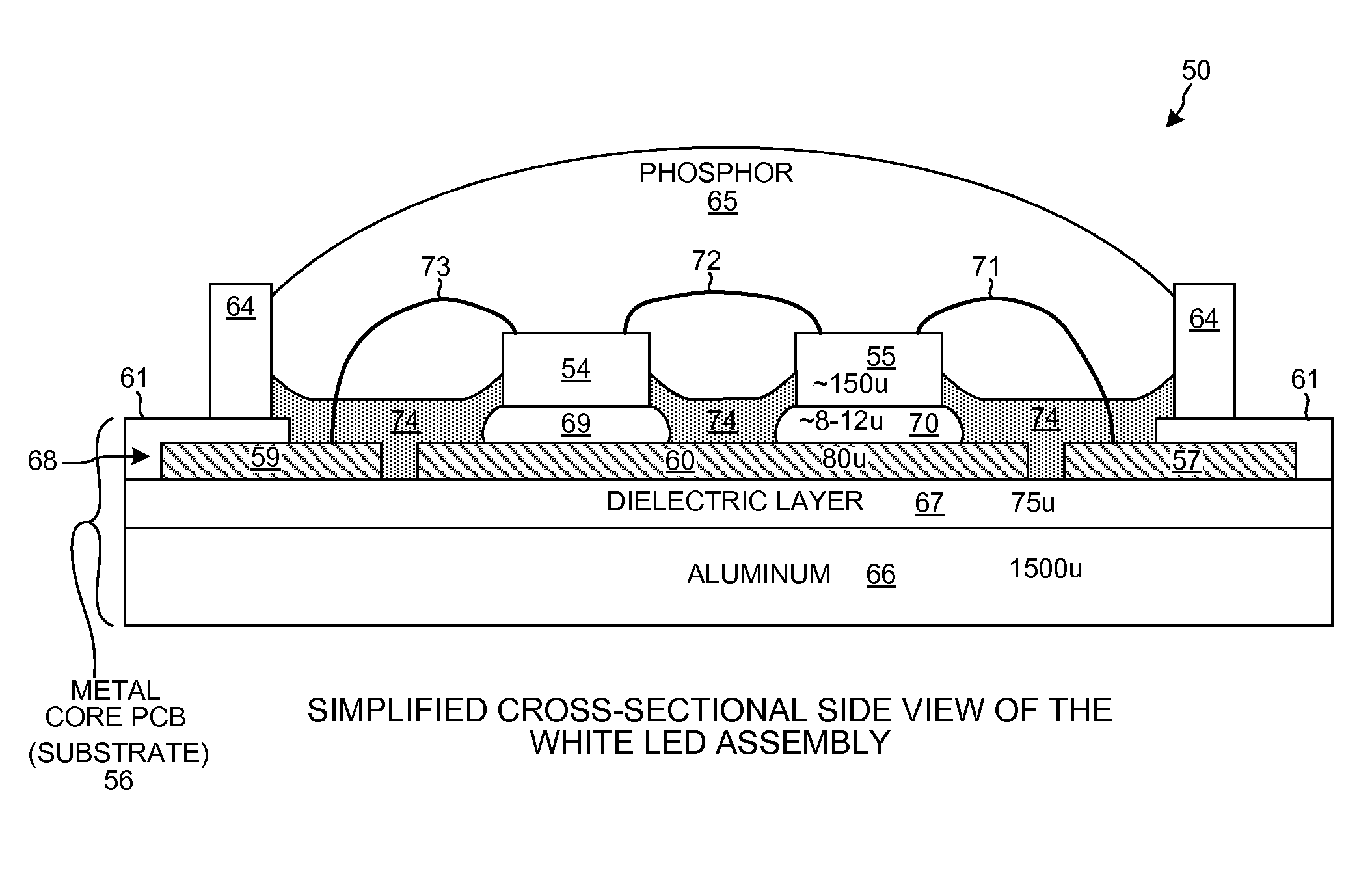
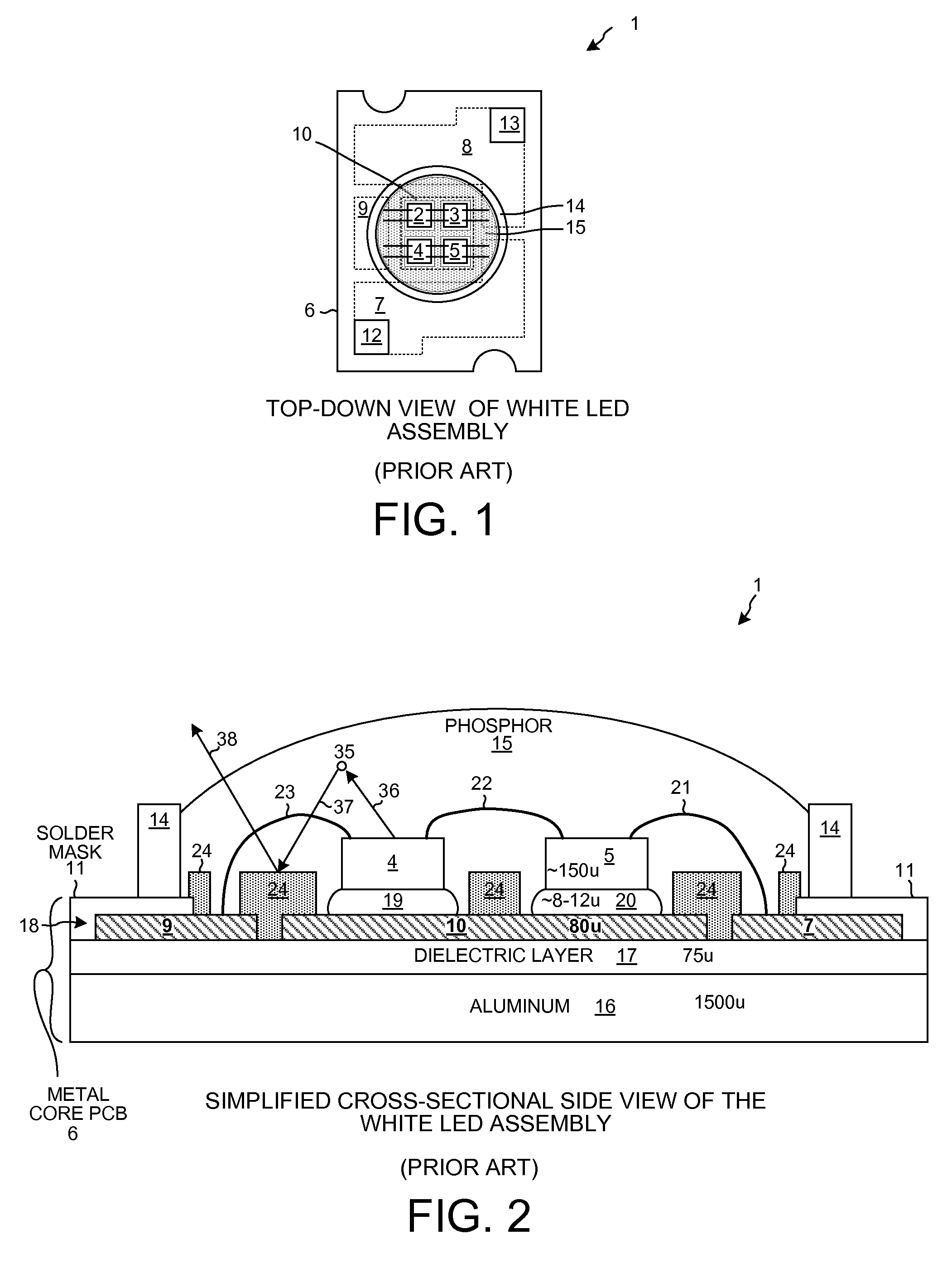
[0036]FIG. 11 is a simplified top-down diagram of a white Light Emitting Diode (LED) assembly 50 in accordance with one novel aspect. LED assembly 50 includes four laterally-contacted LED dice 52-55 that are mounted on a substrate 56. In the present example, the substrate is a Metal Core Printed Circuit Board (MCPCB). Areas 57-60 illustrated in dashed lines represent portions of a metal layer 68 that is disposed underneath a solder mask layer 61 (see FIG. 12). Reference numeral 62 identifies a portion of metal portion 57 that is exposed through a first opening in solder mask layer 61. Reference numeral 63 identifies a portion of metal portion 58 that is exposed through a second opening in solder mask layer 61. These exposed portions 62 and 63 serve as bond pads. Ring structure 64 is a retaining ring of silicone. An amount of phosphor 65 is d...


PUM

PropertyMeasurementUnit
reflectivityaaaaaaaaaa
thickaaaaaaaaaa
diameteraaaaaaaaaa

Abstract

A layer of Highly Reflective (HR) material is deposited by jetting microdots of the HR material in liquid form onto a substrate and then allowing the HR material to harden. In one example, the HR layer is the HR layer of a white LED assembly. The HR layer is jetted onto the substrate around LED dice of the assembly after die attach and wire bonding have been completed. The HR material can be made to flow laterally so that areas of the substrate under wire bonds are coated with HR material, so that HR material contacts side edges of the LED dice, and so that HR material contacts the inside side edge of a retaining ring. By jetting the HR material in this way, the amount of substrate that is not covered with HR material is reduced, thereby improving the light efficiency of the resulting LED assembly.

Description

TECHNICAL FIELD[0001]The present disclosure relates generally to Light Emitting Diode (LED) devices and assemblies and related methods.BACKGROUND INFORMATION[0002]There are many different types of Light Emitting Diode (LED) assemblies. FIG. 1 (Prior Art) is a top-down diagram of one such LED assembly 1. LED assembly 1 includes four laterally-contacted LED dices 2-5 that are mounted on a metal core substrate 6. Substrate 6 in this case is a Metal Core Printed Circuit Board (MCPCB). Areas 7-10 illustrated in dashed lines represent portions of a metal layer that is disposed underneath a solder mask layer 11 (see FIG. 2). Reference numeral 12 identifies a portion of metal portion 7 that is exposed through a first opening in the solder mask layer 11. Similarly, reference numeral 13 identifies a portion of metal portion 8 that is exposed through a second opening in solder mask layer 11. These exposed portions 12 and 13 serve as bond pads. Ring structure 14 is a retaining ring of silicone....

Claims


Application Information

Patent Timeline
Patent Type & Authority Patents(United States)
IPC IPC(8): H01L25/075H01L33/60H01L33/46
CPCH01L25/0753H01L33/46H01L33/60H01L2224/32225H01L2224/45144H01L2224/48137H01L2224/48227H01L2224/73265H01L2224/8592H01L2933/0025H01L2924/00H01L2924/181H01L2924/00012H01L33/502H01L33/62H01L2933/0058H01L2933/0066
Inventor WEST, R. SCOTT
Owner BRIDGELUX INC
Why Eureka
Try Eureka