Method for manufacturing organic light emitting diode display device

a technology of light-emitting diodes and display devices, which is applied in the direction of semiconductor devices, basic electric elements, electrical appliances, etc., can solve the problems of deterioration of thin film transistor performance, non-uniform brightness, and screen staining, so as to prevent deterioration of element performance and minimize hydrogen content

Active Publication Date: 2016-10-04
LG DISPLAY CO LTD
View PDF17 Cites 2 Cited by
  • Summary
  • Abstract
  • Description
  • Claims
  • Application Information

AI Technical Summary

Benefits of technology

[0015]The embodiments are to provide a manufacturing method of an OLED display device which is adapted to prevent deterioration of performance of an element by allowing a passivation layer of a low hydrogen content to cover an OLED with an organic emission layer.
[0016]Also, the embodiments are to provide a manufacturing method of an OLED display device which is adapted to minimize a hydrogen content of a passivation layer covering an OLED with an organic emission layer by forming the passivation layer through polymerization of an organic silicon compound and one of oxygen and nitrogen monoxide.

Problems solved by technology

As such, the performance of the thin film transistor must deteriorate.
As such, faults such as a screen stain and non-uniformity of brightness are generated.

Method used


Image

  • Method for manufacturing organic light emitting diode display device
  • Method for manufacturing organic light emitting diode display device
  • Method for manufacturing organic light emitting diode display device

Examples


Embodiment Construction

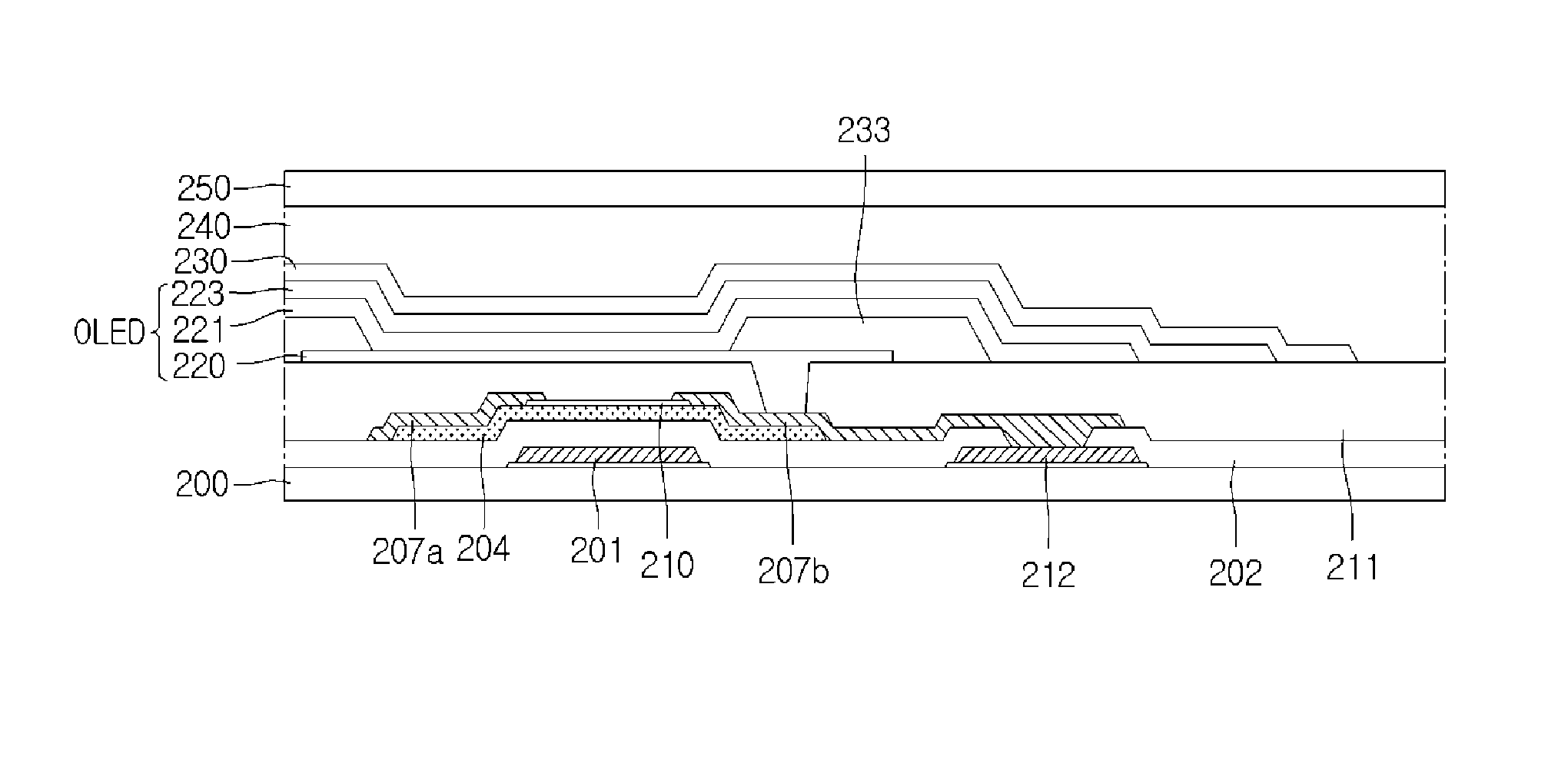
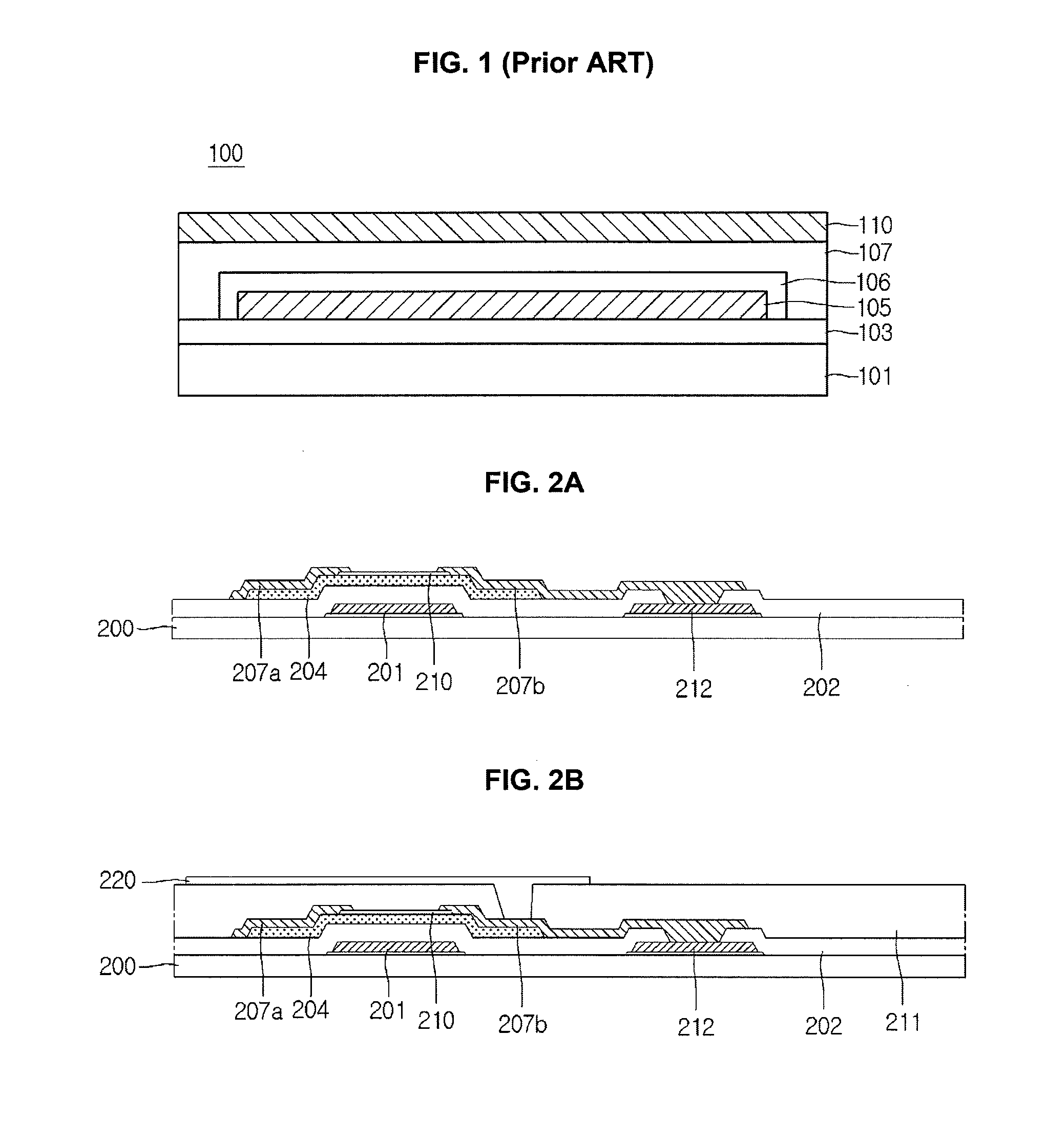
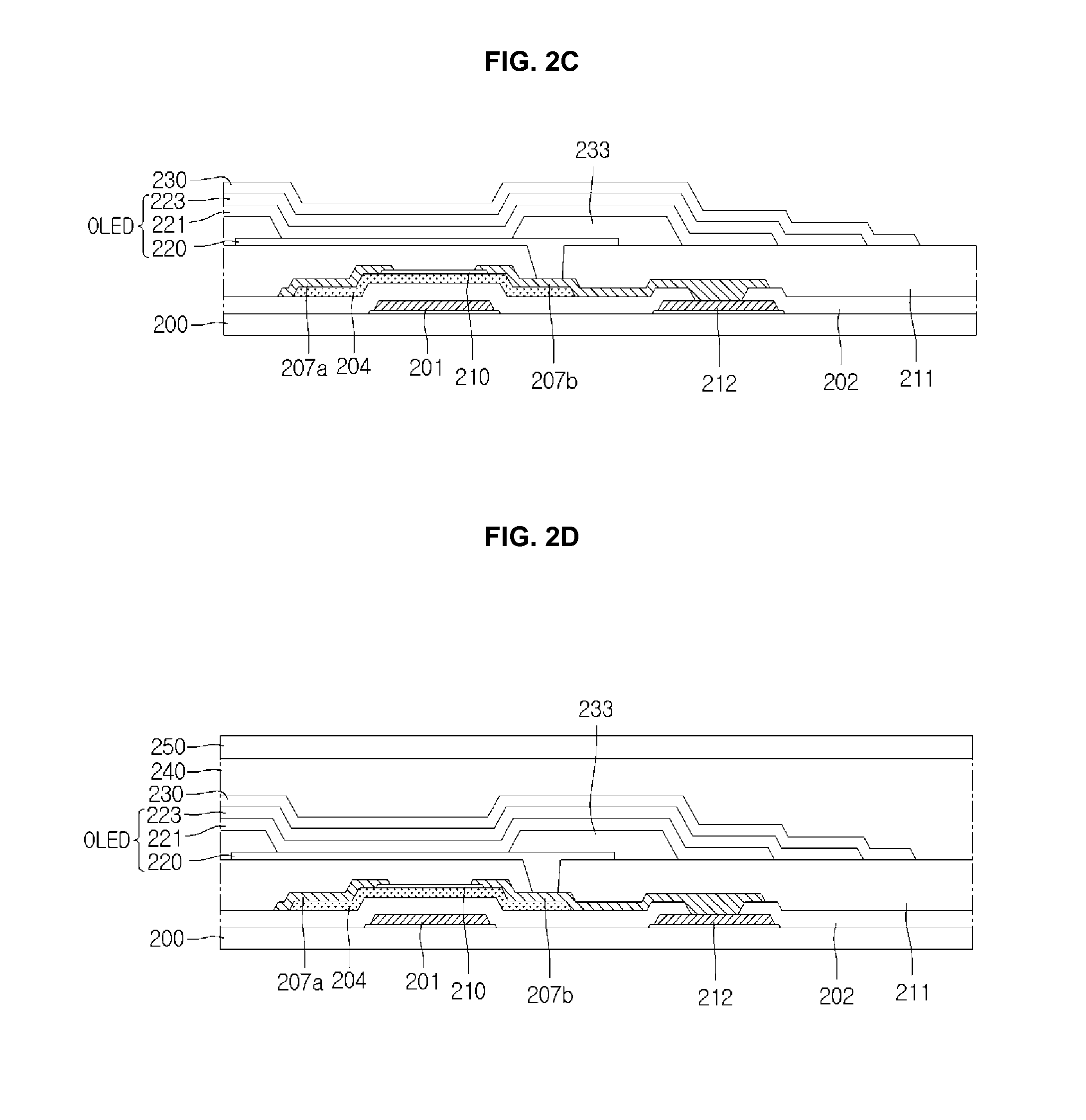
[0029]Reference will now be made in detail to the embodiments of the present invention, examples of which are illustrated in the accompanying drawings. These embodiments introduced hereinafter are provided as examples in order to convey their spirits to the ordinary skilled person in the art. Therefore, these embodiments might be embodied in a different shape, so are not limited to these embodiments described here. Also, the size and thickness of the device might be expressed to be exaggerated for the sake of convenience in the drawings. Wherever possible, the same reference numbers will be used throughout this disclosure including the drawings to refer to the same or like parts.

[0030]FIGS. 2A through 2D are cross-sectional views illustrating a method of manufacturing an OLED display device according to an embodiment of the present disclosure. FIGS. 3A and 3B are diagrams showing structural formulas of organic silicon compounds which are used to form a passivation layer of the OLED ...


PUM


Abstract

A method of manufacturing an OLED device is discussed. The method can include forming a gate electrode on a substrate; forming a gate insulation film on the substrate provided with the gate electrode; forming a channel layer, a source electrode and a drain electrode on the substrate provided with the gate insulation film; forming an organic light emitting diode which includes a first electrode connected to the drain electrode, an organic emission layer formed on the first electrode, and a second electrode formed on the organic emission layer; forming a passivation layer, which has a hydrogen content below 10%, on the substrate provided with the organic light emitting diode using an organic silicon compound; and forming a sealing layer on the substrate provided with the passivation layer.

Description

[0001]The present application claims priority under 35 U.S.C. §119(a) of Korean Patent Application No. 10-2013-0143523 filed on Nov. 25, 2013, which is hereby incorporated by reference in its entirety.BACKGROUND OF THE INVENTION[0002]1. Field of the Disclosure[0003]The present application relates to an organic light emitting diode (OLED) display device. More particularly, the present application relates to a manufacturing method of an organic light emitting display device adapted to enhance the performance of an oxide thin film transistor by reducing a hydrogen content within a passivation layer.[0004]2. Description of the Related Art[0005]Image display devices realizing a variety of information on screens correspond to a core technology of the information communication age. As such, the image display devices are being developed in such a manner as to be more thin and light and portable and have high performance. Moreover, flexible display devices are being required in order to enha...

Claims


Application Information

Patent Timeline
Patent Type & Authority Patents(United States)
IPC IPC(8): H01L51/52H01L27/12
CPCH01L51/5253H01L27/1225H10K59/873H10K50/844
Inventor KANG, JIN GOOSHIN, YOUNG HOON
Owner LG DISPLAY CO LTD
Why Eureka
Try Eureka