Multilayer wiring substrate

a multi-layer wiring and substrate technology, applied in the direction of printed circuit stress/warp reduction, printed circuit aspects, semiconductor/solid-state device details, etc., can solve the problems of multi-layer wiring substrate cracking, flatness of the upper surface and the lower surface etc., to suppress the cracking the degradation of surface flatness, the effect of effectively suppressing the warping of multi-layer wiring substrates

Active Publication Date: 2016-10-11
MURATA MFG CO LTD
View PDF45 Cites 0 Cited by
  • Summary
  • Abstract
  • Description
  • Claims
  • Application Information

AI Technical Summary

Benefits of technology

[0008]An object of the present invention is to provide a multilayer wiring substrate, which is less apt to cause the warping and to degrade the surface flatness, and which can effectively suppress the occurrence of cracks.
[0023]With the multilayer wiring substrate according to the present invention, the wiring formed in the substrate body includes the wiring conductor having the nonlinear shape. It is hence possible to effectively suppress the warping of the multilayer wiring substrate and the degradation of the surface flatness thereof. Moreover, an impact exerted from the outside can be relieved, and the occurrence of cracks in the multilayer wiring substrate can be suppressed effectively.

Problems solved by technology

Another problem is that the flatness of the upper surface and the lower surface of the multilayer wiring substrate is apt to degrade.
This raises the problem that the multilayer wiring substrate tends to crack.

Method used


Image

  • Multilayer wiring substrate
  • Multilayer wiring substrate
  • Multilayer wiring substrate

Examples


first embodiment

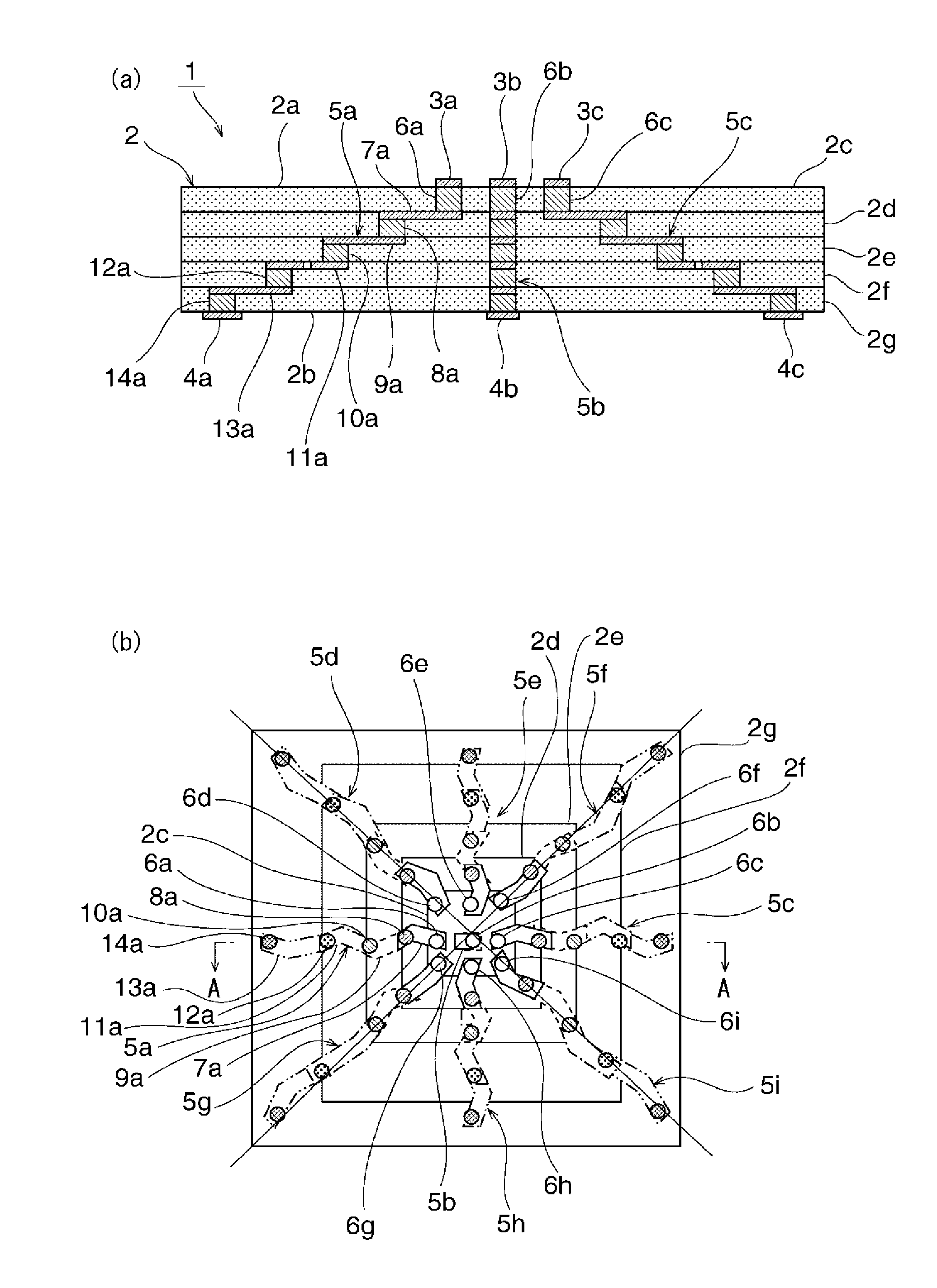
[0040]FIG. 1(a) is a schematic front sectional view of a multilayer wiring substrate according to the present invention, and FIG. 1(b) is a schematic plan view illustrating, in simplified representation, a plurality of wirings formed inside the multilayer wiring substrate.

[0041]As illustrated in FIG. 1(a), a multilayer wiring substrate 1 includes a substrate body 2. The substrate body 2 has a first principal surface 2a and a second principal surface 2b that is a surface positioned on the side opposite to the first principal surface 2a. The first principal surface 2a serves as a mount surface on which an electronic component, such as an IC chip, a measurement probe card and so on are mounted. Accordingly, a plurality of electrodes 3a to 3c are formed on the first principal surface 2a.

[0042]A plurality of terminal electrodes 4a to 4c are formed on the second principal surface 2b. The plural terminal electrodes 4a to 4c are arranged at a lower density than the plural electrodes 3a to ...

fourth embodiment

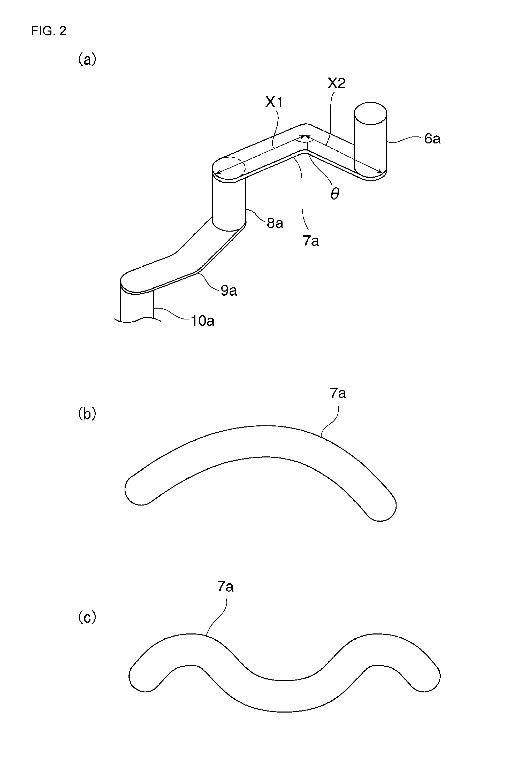
[0094]FIG. 12 is a schematic front sectional view illustrating principal part of a multilayer wiring substrate according to a modification of the present invention. Also in this modified embodiment, as illustrated in FIG. 12, a gap 51 is formed between the via conductor 8a disposed in the second insulator layer 2d and the second insulator layer 2d. The via conductor 8a has a substantially trapezoidal shape in section. In other words, the sectional shape of the via conductor is not limited to particular one.

[0095]FIG. 13 is a schematic front sectional view to explain a multilayer wiring substrate according to a fifth embodiment of the present invention. The fifth embodiment corresponds to a modification of the embodiment illustrated in FIG. 11. In the fifth embodiment, a wiring 5a includes via conductors 6a, 8a, 10a, 12a, 14a and 16a that are arranged as illustrated. Stated in another way, the wiring 5a is flexed as denoted by an imaginary line P. A gap 51 is formed around the via co...


PUM


Abstract

A multilayer wiring substrate is provided which is less apt to cause the warping and the degradation of the surface flatness, and which is able to effectively suppress the occurrence of cracks. A multilayer wiring substrate 1 includes a substrate body 2 in which a plurality of wirings 5a are disposed to extend from a first principal surface 2a toward a second principal surface 2b. The wiring 5a or 5b includes via conductors 6a and 8a disposed respectively in at least two insulator layers in which the wiring is disposed, a wiring conductor 7a connecting the via conductor 6a, which is disposed in one 2c of the insulator layers adjacent to each other in a stacking direction of the insulator layers, and the via conductor 8a disposed in the other insulator layer 2d, the wiring conductor 7a having a nonlinear shape.

Description

BACKGROUND OF THE INVENTION[0001]1. Field of the Invention[0002]The present invention relates to a multilayer wiring substrate in which a plurality of wirings, including via conductors and wiring conductors, is formed inside a substrate body.[0003]2. Description of the Related Art[0004]Hitherto, a multilayer wiring substrate has been used as a substrate on which a semiconductor element, such as an IC, is to be mounted. Outer terminals of the semiconductor element are arranged at a higher density with an increasing degree of integration. In view of such a situation, Patent Document 1 and Patent Document 2, given below, disclose multilayer wiring substrates each including a plurality of electrodes formed at a high density on an upper surface thereof on which a semiconductor element etc. are mounted. In those multilayer wiring substrates, a plurality of outer electrodes arranged at a relatively wide pitch is formed on a lower surface of the substrate. Those plural outer electrodes are ...

Claims


Application Information

Patent Timeline
Patent Type & Authority Patents(United States)
IPC IPC(8): H05K1/11H05K1/02H01L23/498H05K3/46
CPCH05K1/115H01L23/49822H01L23/49827H01L23/49838H05K1/0271H05K1/0298H05K3/4629H01L2924/0002H01L2924/15174H05K2201/09227H05K2201/09272H05K2201/09709H01L2924/00012
Inventor OTSUBO, YOSHIHITO
Owner MURATA MFG CO LTD
Why Eureka
Try Eureka