Forming a semiconductor structure for reduced negative bias temperature instability

a technology of temperature instability and semiconductor structure, applied in the field of semiconductor technology, can solve the problems of adversely affecting the stability of transistors formed with thinner gate dielectric materials, the scaling of the semiconductor device to smaller feature sizes is facing significant challenges, and the traditional semiconductor materials and process for device formation become less effective, so as to improve the negative bias temperature instability

Inactive Publication Date: 2016-11-22
IBM CORP
View PDF12 Cites 17 Cited by
  • Summary
  • Abstract
  • Description
  • Claims
  • Application Information

AI Technical Summary

Benefits of technology

[0004]Embodiments of the present invention provide a method of forming a semiconductor structure with improved negative bias temperature instability. The method includes forming an interfacial layer on a semiconductor substrate with an nFET and a pFET. The method includes depositing a gate dielectric layer on the interfacial layer. Additionally, the gate dielectric layer is covered by a deposited layer of an nFET work function metal. The method includes removing the nFET work function metal from an area above the pFET where the area above the...

Problems solved by technology

Semiconductor device scaling to smaller feature sizes is facing significant challenges.
Traditional semiconductor materials and processes for device formation become less effective as physical dimensions shrink down to the nanometer regime.
As gate layers become thinner, a number of issues arise.
Time-related voltage breakdowns, hot carrier effects, and diffusion of impurities from the gate electrode to the substrate may occur which can adversely affect the stability of transistors formed with thinner gate dielectric materials.
Neg...

Method used


Image

  • Forming a semiconductor structure for reduced negative bias temperature instability
  • Forming a semiconductor structure for reduced negative bias temperature instability
  • Forming a semiconductor structure for reduced negative bias temperature instability

Examples


Embodiment Construction

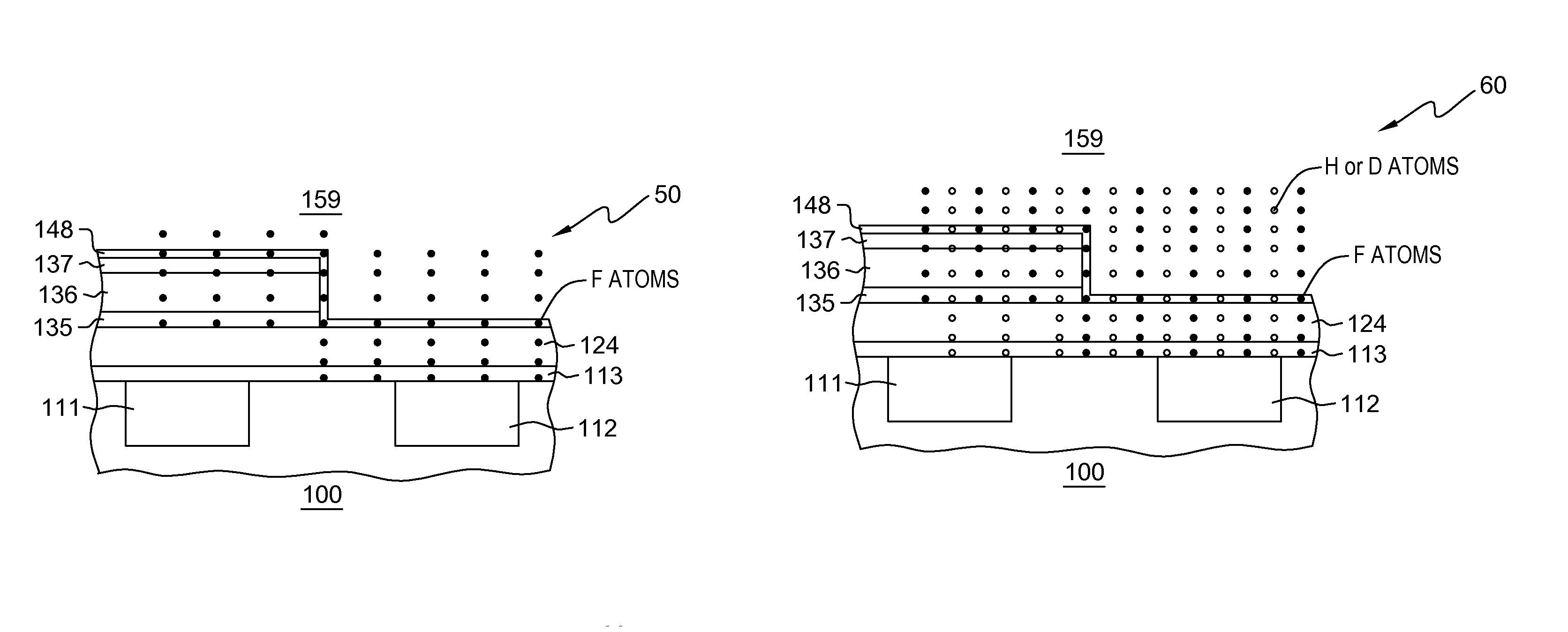
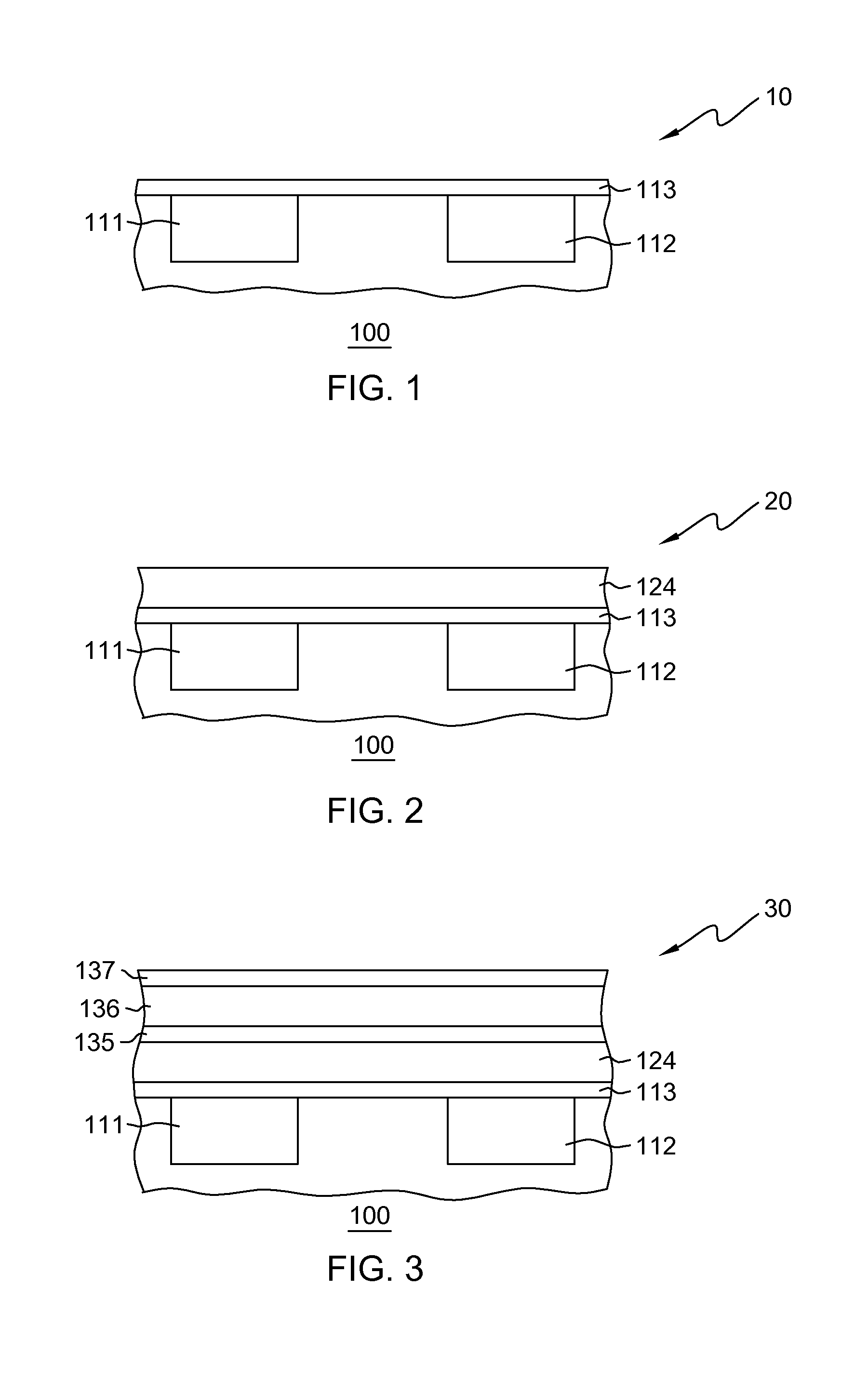
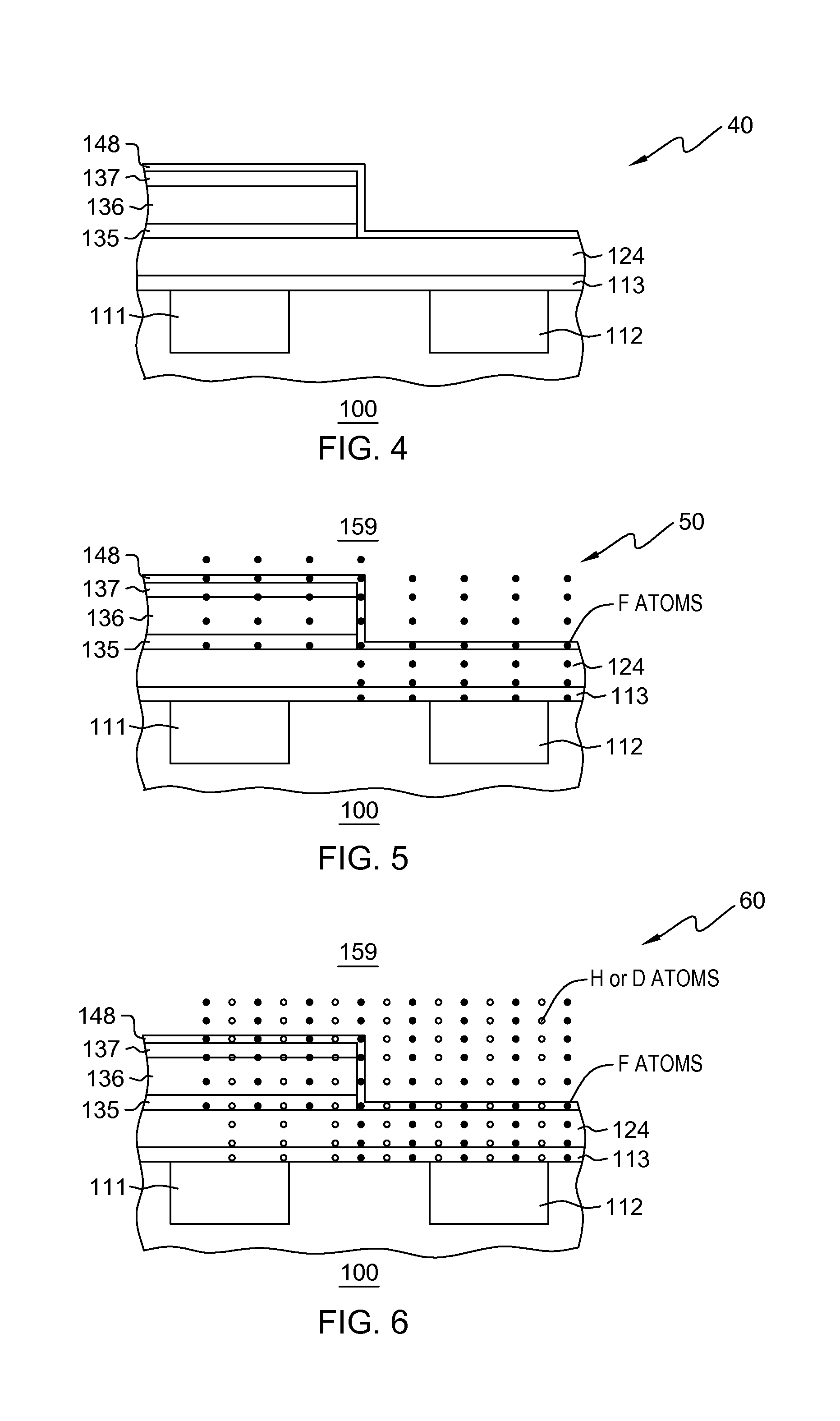
[0020]Detailed embodiments of the claimed structures and methods are disclosed herein. The method steps described below do not form a complete process flow for manufacturing integrated circuits. The present embodiments can be practiced in conjunction with the integrated circuit fabrication techniques currently used in the art, and only so much of the commonly practiced process steps are included as are necessary for an understanding of the described embodiments. The figures represent cross-section portions of a semiconductor chip or a semiconductor wafer during fabrication and are not drawn to scale, but instead are drawn to illustrate the features of the described embodiments. Specific structural and functional details disclosed herein are not to be interpreted as limiting, but merely as a representative basis for teaching one skilled in the art to variously employ the methods and structures of the present disclosure. In the description, details of well-known features and technique...


PUM


Abstract

An approach to forming a semiconductor structure with improved negative bias temperature instability includes forming an interfacial layer on a semiconductor substrate with an nFET and a pFET. The approach includes depositing a gate dielectric layer on the interfacial layer. Additionally, the approach includes an nFET work function metal layer deposited on the interfacial layer. Additionally, the approach includes removing the nFET work function metal from an area above the pFET and depositing a pFET work function metal layer on a portion of the exposed gate dielectric layer where the portion of the exposed gate dielectric layer is over the pFET. Furthermore, the approach includes depositing a gate metal on the pFET work function metal layer where the gate metal is deposited in an environment with a fluorine containing gas followed by an anneal in a reducing environment.

Description

BACKGROUND OF THE INVENTION[0001]The present invention relates generally to the field of semiconductor technology, and more particularly to semiconductor manufacture.[0002]Semiconductor device scaling to smaller feature sizes is facing significant challenges. Traditional semiconductor materials and processes for device formation become less effective as physical dimensions shrink down to the nanometer regime. With this reduction in feature size, the thickness of gate dielectrics layers has continually decreased. As gate layers become thinner, a number of issues arise. Time-related voltage breakdowns, hot carrier effects, and diffusion of impurities from the gate electrode to the substrate may occur which can adversely affect the stability of transistors formed with thinner gate dielectric materials. The migration to high-k gate dielectric materials that improve gate current density for a similar effective oxide thickness may be done for improved electrical performing in shrinking de...

Claims


Application Information

Patent Timeline
IPC IPC(8): H01L21/8238H01L29/66H01L29/49H01L29/51H01L27/092
CPCH01L21/823842H01L29/66545H01L29/4966H01L29/517H01L27/0922H01L29/513H01L21/28088H01L21/28176H01L21/3003H01L27/092H01L21/823857H01L21/28556H01L21/823828H01L29/42364H01L29/42372H01L29/4958H01L21/3115H01L21/3215H01L21/82385
Inventor BAO, RUQIANGKRISHNAN, SIDDARTH A.
Owner IBM CORP
Why Eureka
Try Eureka