Memory element and signal processing circuit

a signal processing circuit and memory element technology, applied in the field of memory element and signal processing circuit, can solve the problems of limited rewriting time, writing error, limited rewriting time, etc., and achieve the effects of reducing the frequency of rewritable times, reducing the degradation of the element, and increasing the number of rewritable times of data

Active Publication Date: 2016-11-29
SEMICON ENERGY LAB CO LTD
View PDF171 Cites 4 Cited by
  • Summary
  • Abstract
  • Description
  • Claims
  • Application Information

AI Technical Summary

Benefits of technology

[0018]The memory element can further include a sense amplifier and a precharge circuit. The precharge circuit can include a first switch, a second switch, and a wiring (or a terminal) to which a precharge potential is applied. The other of the source and the drain of the second transistor and the other of the source and the drain of the fourth transistor are electrically connected to each other and electrically connected to an input terminal of the sense amplifier via the first switch. In addition, the wiring to which the precharge potential is applied is electrically connected to the input terminal of the sense amplifier via the second switch. Then, the sense amplifier amplifies and outputs a potential which is input to the input terminal. Note that the sense amplifier may output a result of a comparison between a reference potential and the potential which is input to the input terminal. With the output of the sense amplifier, the first signal or the second signal can be read out. As the sense amplifier, for example, an inverter, a clocked inverter, a buffer, a latch circuit, an operational amplifier, or the like can be used. When the precharge circuit is provided, the first switch is turned off and the second switch is turned on so that the input terminal of the sense amplifier can have a precharge potential, and then the first switch is turned on and the second switch is turned off so that the potential of the input terminal of the sense amplifier can be set at a predetermined potential corresponding to stored data. Thus, a time until the potential of the input terminal of the sense amplifier is set at the predetermined potential corresponding to the stored data can be shortened. As a result, the data stored in the memory element can be read out speedily.(Specific Example 2)
[0043]The use of the memory element in a signal processing circuit allows the signal processing circuit to hold data for a long time even after the supply of the power supply voltage is stopped. Thus, when supply of a power supply voltage restarts, the signal processing circuit can immediately start predetermined processing using the stored data. Therefore, stop of the power supply for a short time can be performed frequently in the signal processing circuit, so that power consumption can be further reduced. In addition, as described above, it is possible to increase the number of rewritable times of data, and when the memory element in which writing errors and reading errors of data hardly occur is used in the signal processing circuit, the reliability of the signal processing circuit can be improved. In addition, as described above, the use of the memory element whose writing speed is high in the signal processing circuit makes it possible to also improve the operation speed of the signal processing circuit.

Problems solved by technology

In the memory element including a ferroelectric, a ferroelectric material is fatigued by repetition of data writing, which causes a problem such as a writing error.
As a result, the number of rewriting times is limited.
Therefore, there are problems such that memory elements intensively deteriorate by repeatedly performing data rewriting, so that the number of rewriting times is limited.
In the case where data of a volatile memory device is stored in an external memory device while supply of a power supply voltage is stopped in the signal processing circuit, it takes a long time until the data is returned from the external memory device to the volatile memory device.
Therefore, such a signal processing circuit is not suitable for a short-time stop of power supply for the purpose of a reduction in power consumption.

Method used


Image

  • Memory element and signal processing circuit
  • Memory element and signal processing circuit
  • Memory element and signal processing circuit

Examples


embodiment 1

(Embodiment 1)

(Structure 1 of Memory Element)

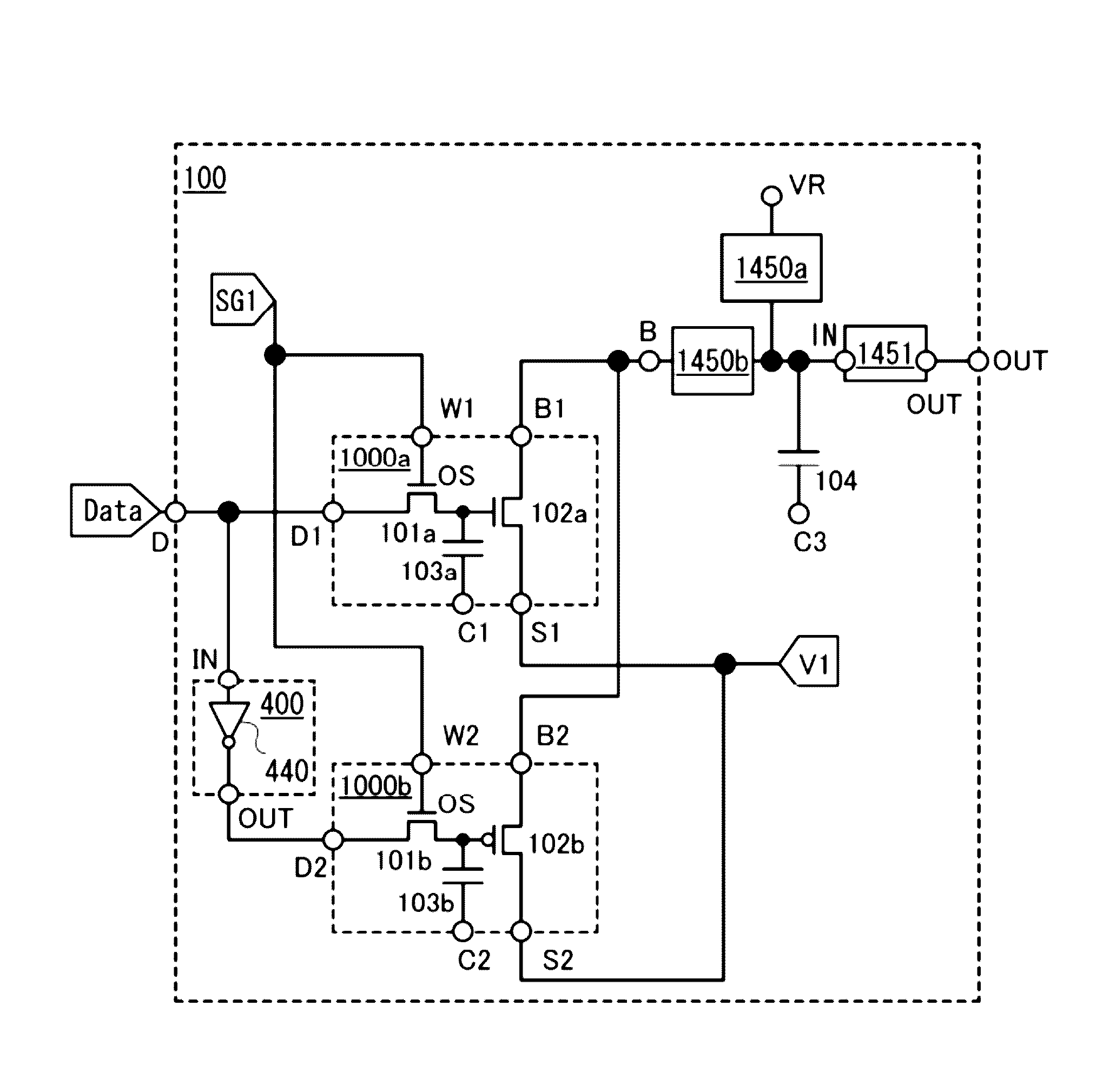
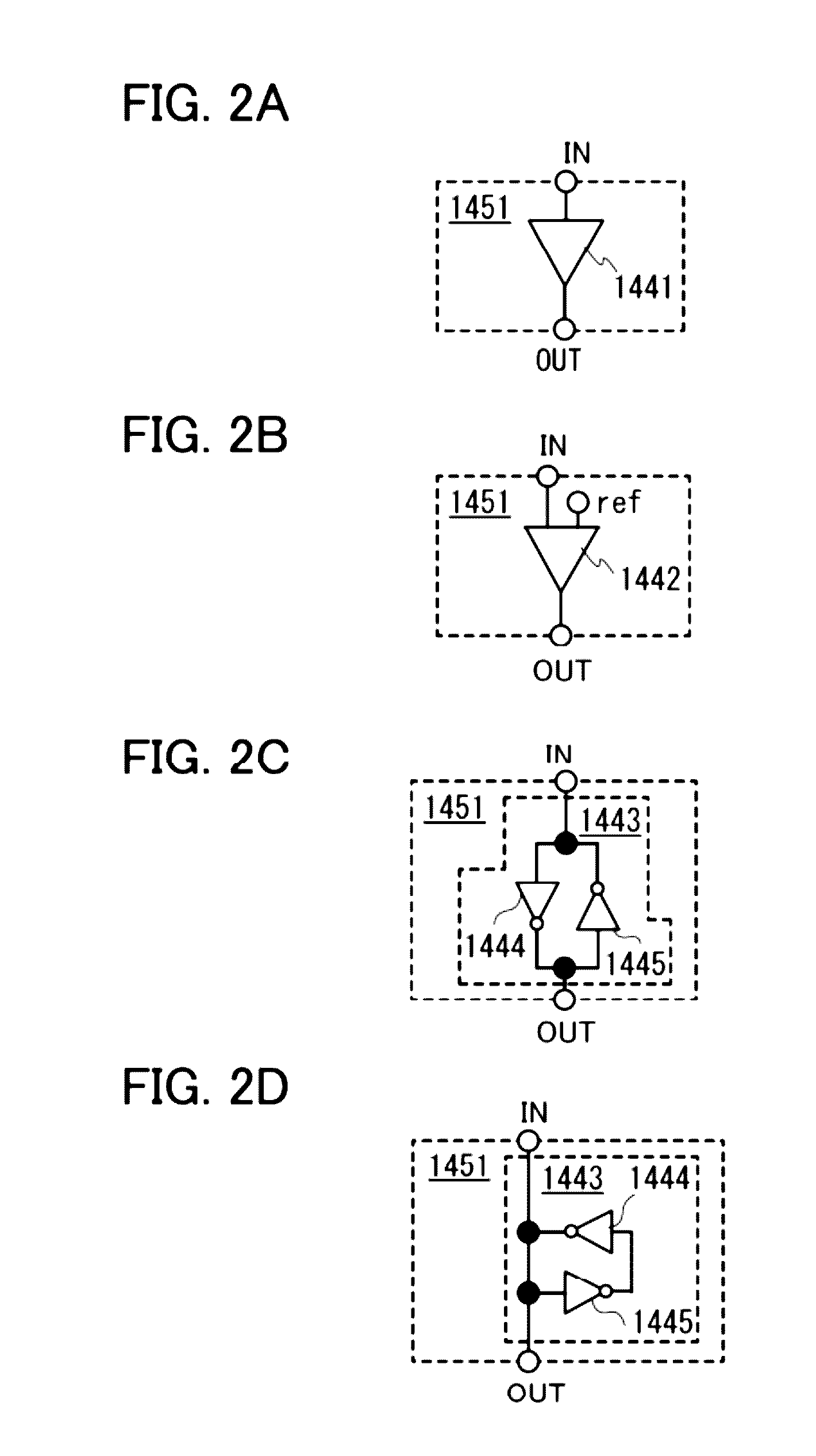
[0088]FIG. 1 illustrates a memory element that is one embodiment of the present invention. In FIG. 1, a memory element 100 includes a circuit 1000a, a circuit 1000b, an inverter circuit 400, a sense amplifier 1451, a switch 1450a, a switch 1450b, and a capacitor 104. Data is input to a terminal D, and the memory element 100 holds a signal corresponding to the data and outputs the signal corresponding to the data from a terminal OUT. The circuit 1000a includes a transistor 101a, a transistor 102a, and a capacitor 103a. The circuit 1000b includes a transistor 101b, a transistor 102b, and a capacitor 103b. Note that one or all of the capacitor 103a, the capacitor 103b, and the capacitor 104 can be omitted by positively using a parasitic capacitance or the like.

[0089]In the circuit 1000a, a gate of the transistor 101a is electrically connected to a terminal W1, one of a source and a drain of the transistor 101a is electrically connected to a ...

embodiment 2

(Embodiment 2)

(Structure 2 of Memory Element)

[0115]FIG. 8 illustrates a memory element that is another embodiment of the present invention. In FIG. 8, a memory element 100 includes a circuit 1000a, a circuit 1000b, a sense amplifier 1451, a switch 8450a, a switch 8450b, a capacitor 104a, a switch 9450a, a switch 9450b, and a capacitor 104b. Data is input to a terminal D, and the memory element 100 holds a signal corresponding to the data and outputs the signal corresponding to the data from a terminal OUT. The circuit 1000a includes a transistor 101a, a transistor 102a, and a capacitor 103a. The circuit 1000b includes a transistor 101b, a transistor 102b, and a capacitor 103b. Note that one or all of the capacitor 103a, the capacitor 103b, the capacitor 104a, and the capacitor 104b can be omitted by positively using a parasitic capacitance or the like.

[0116]In the circuit 1000a, a gate of the transistor 101a is electrically connected to a terminal W1, one of a source and a drain of ...

embodiment 3

(Embodiment 3)

(Structure 3 of Memory Element)

[0141]FIG. 13 illustrates a memory element that is another embodiment of the present invention. In FIG. 13, a memory element 100 includes a circuit 1000a, a circuit 1000b, an inverter circuit 400, a sense amplifier 1451, a switch 8450a, a switch 8450b, a capacitor 104a, a switch 9450a, and a capacitor 104b. Data is input to a terminal D, and the memory element 100 holds a signal corresponding to the data and outputs the signal corresponding to the data from a terminal OUT. The circuit 1000a includes a transistor 101a, a transistor 102a, and a capacitor 103a. The circuit 1000b includes a transistor 101b, a transistor 102b, and a capacitor 103b. Note that one or all of the capacitor 103a, the capacitor 103b, the capacitor 104a, and the capacitor 104b can be omitted by positively using a parasitic capacitance or the like.

[0142]In the circuit 1000a, a gate of the transistor 101a is electrically connected to a terminal W1, one of a source and ...


PUM


Abstract

A memory element having a novel structure and a signal processing circuit including the memory element are provided. A first circuit, including a first transistor and a second transistor, and a second circuit, including a third transistor and a fourth transistor, are included. A first signal potential and a second signal potential, each corresponding to an input signal, are respectively input to a gate of the second transistor via the first transistor in an on state and to a gate of the fourth transistor via the third transistor in an on state. After that, the first transistor and the third transistor are turned off. The input signal is read out using both the states of the second transistor and the fourth transistor. A transistor including an oxide semiconductor in which a channel is formed can be used for the first transistor and the third transistor.

Description

BACKGROUND OF THE INVENTION[0001]1. Field of the Invention[0002]The present invention relates to a memory element, and to a memory device and a signal processing circuit including the memory element. Furthermore, the present invention relates to an electronic device including the signal processing circuit.[0003]2. Description of the Related Art[0004]A signal processing circuit such as a central processing unit (CPU) has a variety of configurations depending on its application but is generally provided with some kinds of memory devices such as a register and a cache memory as well as a main memory for storing data or a program. A register has a function of temporarily holding data for carrying out arithmetic processing, holding a program execution state, or the like. In addition, a cache memory is located between an arithmetic circuit and a main memory in order to reduce low-speed access to the main memory and speed up the arithmetic processing.[0005]In a storage device such as a reg...

Claims


Application Information

Patent Timeline
Patent Type & Authority Patents(United States)
IPC IPC(8): G11C11/40G11C19/28G11C19/18G11C16/04
CPCG11C19/28G11C19/184G11C16/0441G06F1/00G11C7/06G11C7/10G11C7/12G11C14/0054
Inventor ENDO, MASAMI
Owner SEMICON ENERGY LAB CO LTD
Why Eureka
Try Eureka