Organic material resistance random access memory element and manufacturing method thereof

A technology of resistive memory and organic materials, applied in the fields of electrical components, semiconductor/solid-state device manufacturing, electric solid-state devices, etc., can solve the problems of unsuitability for commercial applications and unstable performance parameters of resistive memory.

Active Publication Date: 2015-12-23
HEBEI UNIVERSITY
View PDF3 Cites 12 Cited by
  • Summary
  • Abstract
  • Description
  • Claims
  • Application Information

AI Technical Summary

Problems solved by technology

[0004] One of the purposes of the present invention is to provide a resistive memory element based on organic materials to solve the problem that the existing resistive memory has unstable performance parameters and is not suitable for commercial application

Method used


Image

  • Organic material resistance random access memory element and manufacturing method thereof
  • Organic material resistance random access memory element and manufacturing method thereof
  • Organic material resistance random access memory element and manufacturing method thereof

Examples


Embodiment 1

[0023] Embodiment 1, an organic material resistive memory element.

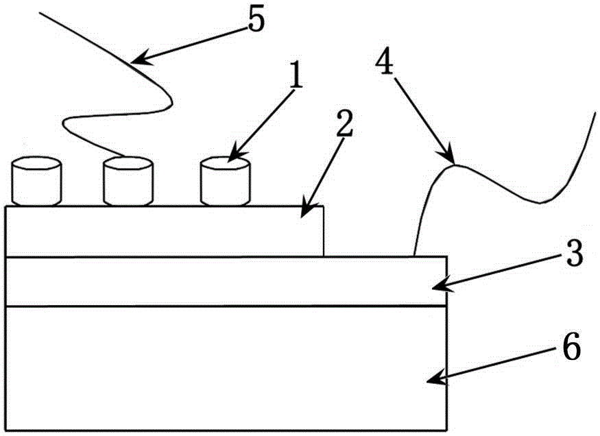
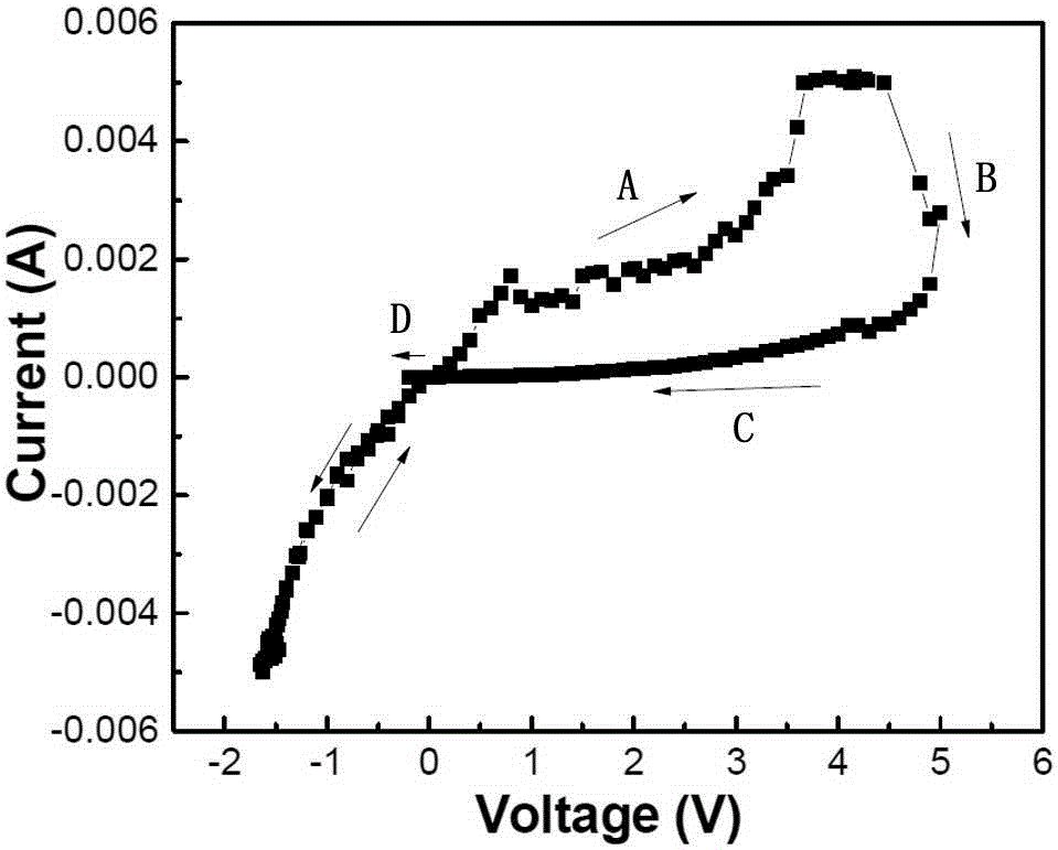
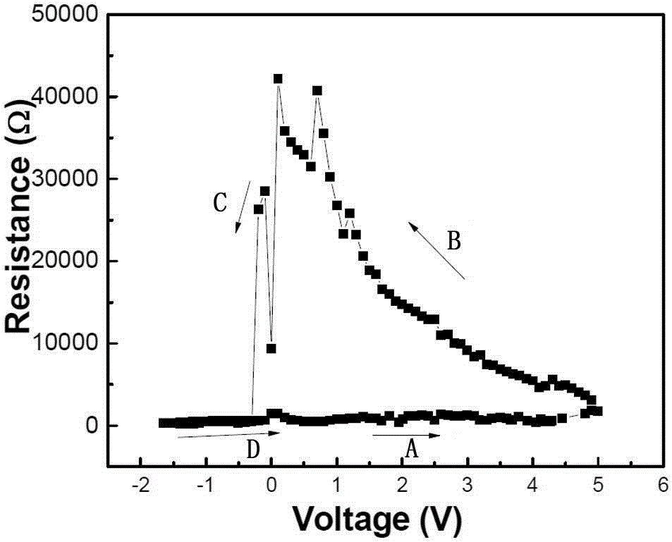
[0024] Such as figure 1 As shown, the structure of the organic material resistive memory element in the present invention includes a lower electrode layer 3, a resistive medium layer 2 and an upper electrode layer 1 arranged in sequence from bottom to top; the lower electrode layer 3 is an ITO (indium tin oxide) layer , the ITO layer can generally be attached to the glass 6 by magnetron sputtering, that is, when preparing the organic material resistive memory element in the present invention, it can be used as The substrate, ITO glass, provides the lower electrode layer 3 . The thickness of the ITO layer on the ITO glass may be 10 nm to 500 nm. The resistive dielectric layer 2 is CH 3 NH 3 PB 3?x Cl 3 layer, the thickness of the resistive medium layer 2 can be set to 10nm-500nm, preferably, can be set to 30nm-200nm. The upper electrode layer 1 is generally composed of several evenly distributed circula...

Embodiment 2

[0026] Embodiment 2, a method for preparing an organic material resistive memory element.

[0027] The preparation method of the organic material resistive memory element in this embodiment includes the following steps:

[0028] a. Select ITO glass as the substrate, the ITO layer on the substrate is the lower electrode layer, and the thickness of the ITO layer is 200nm. Pretreatment of ITO glass: put the ITO glass in acetone and ultrasonically clean it for 1 minute, then put it in alcohol and clean it with ultrasonic wave for 1 minute, then put it in deionized water and clean it with ultrasonic wave for 5 minutes, then take it out and use high-purity ( Purity of 99.99% and above) nitrogen (N 2 ) and blow dry.

[0029] b. Fix the ITO glass pretreated in step a on the spin coater in the glove box, fill the glove box with high-purity (purity of 99.99% and above) nitrogen, and fill the glove box with 0.14 mol / L of PbCl 2 solution, 1.26mol / L of PbI 2 Solution and 1.3mol / L meth...

Embodiment 3

[0037] Embodiment 3, a method for preparing an organic material resistive memory element.

[0038] The method for preparing an organic material resistive memory element in this embodiment also includes four steps a, b, c, and d, wherein, steps a, b, and c are all the same as the corresponding steps in embodiment 2, the difference is Step d, the step d in the present embodiment is as follows:

[0039] d, form CH in step c 3 NH 3 PB 3?x Cl 3 layer and annealed ITO glass is placed on the target platform in the vacuum evaporation growth chamber, and a mask is placed on it. The mask is evenly distributed with 100 μm round holes, and an Al target is placed above the mask. , the vacuum evaporation growth chamber was evacuated to 3×10 -4 Pa, set the sputtering power to 10W, the sputtering distance to 6cm, the sputtering time to 8min, and the rate of 13nm / min in CH 3 NH 3 PB 3?x Cl 3 An Al upper electrode layer with a thickness of about 100nm is deposited on the layer, and the...


PUM

PropertyMeasurementUnit
thicknessaaaaaaaaaa
thicknessaaaaaaaaaa
diameteraaaaaaaaaa

Abstract

The invention provides an organic material resistance random access memory element and a manufacturing method thereof. The structure of the memory element comprises a lower electrode layer, a resistance random dielectric layer, and an upper electrode layer arranged in sequence from bottom to top. The lower electrode layer is an ITO layer. The resistance random dielectric layer is CH3NH3PbI(3-x)Cl3 layer. The upper electrode layer is an Ag layer or an Al layer. The manufacturing method for the organic material resistance random access memory element comprises: using a sol-gel method to form the CH3NH3PbI(3-x)Cl3 layer on the ITO layer of ITO glass, and then performing annealing treatment, and then using a vacuum evaporation method to deposit Ag or Al upper electrode layer on the CH3NH3PbI(3-x)Cl3 layer, and finally a resistance random access memory element whose heterostructure form is Ag or Al/CH3NH3PbI(3-x)Cl3/ITO is formed. The organic material resistance random access memory element is stable in performance, and has relatively good fatigue resistance and holding property.

Description

technical field [0001] The invention relates to a semiconductor memory, in particular to a resistive memory element with an organic material as a storage medium and a preparation method thereof. Background technique [0002] With the improvement of the semiconductor process level and the continuous development of the information industry, semiconductor devices have gradually reached the limits of physics and technology. The key to meeting this challenge lies in finding new materials and developing new device structures. Non-volatile memory plays an increasingly important role in the development of integrated circuits. At present, flash memory (Flash memory) is the mainstream of non-volatile memory (NVM) on the market, but this type of memory has low read and write speeds and short switch life, and cannot be used for main storage components that require frequent reads and writes in computers, and its The storage mechanism is based on the charge storage mechanism. Therefore,...

Claims


Application Information

Patent Timeline
Patent Type & Authority Applications(China)
IPC IPC(8): H01L51/05H01L51/30H01L51/40
CPCH10K71/12H10K85/341H10K10/701
Inventor 闫小兵
Owner HEBEI UNIVERSITY
Why Eureka
Try Eureka