Oscillation circuit

a technology of oscillating circuits and oscillating components, applied in oscillating generators, pulse techniques, pulse generators, etc., can solve problems such as difficulty in preventing functional circuits from causing operational problems

Active Publication Date: 2016-12-20
LAPIS SEMICON CO LTD
View PDF9 Cites 0 Cited by
  • Summary
  • Abstract
  • Description
  • Claims
  • Application Information

AI Technical Summary

Benefits of technology

[0012]According to the first aspect of the present invention, the electrical current control portion includes an input terminal connected to the control voltage generating portion for receiving the electrical current; a control terminal connected to the control voltage generating portion for receiving the control voltage; and an output terminal. Further, the electrical current control portion is configured to reduce the amplitude of the electrical current flowing between the input terminal and the output terminal as the magnitude of the control voltage is decreased.
[0015]According to the present invention, it is possible to provide the oscillation circuit capable of preventing a functional circuit from causing an operational problem when the oscillation circuit is provided for supplying a clock signal to the functional circuit, even if the functional circuit tends to delay in following the clock signal when the power source voltage is decreased.

Problems solved by technology

If this happens, the functional circuit is not able to operate in synchronization with the clock signal, thereby causing an operational problem.
However, in this case, if the start timing of the frequency division is delayed, it is difficult to prevent the functional circuit from causing the operational problem.

Method used


Image

  • Oscillation circuit
  • Oscillation circuit
  • Oscillation circuit

Examples


first embodiment

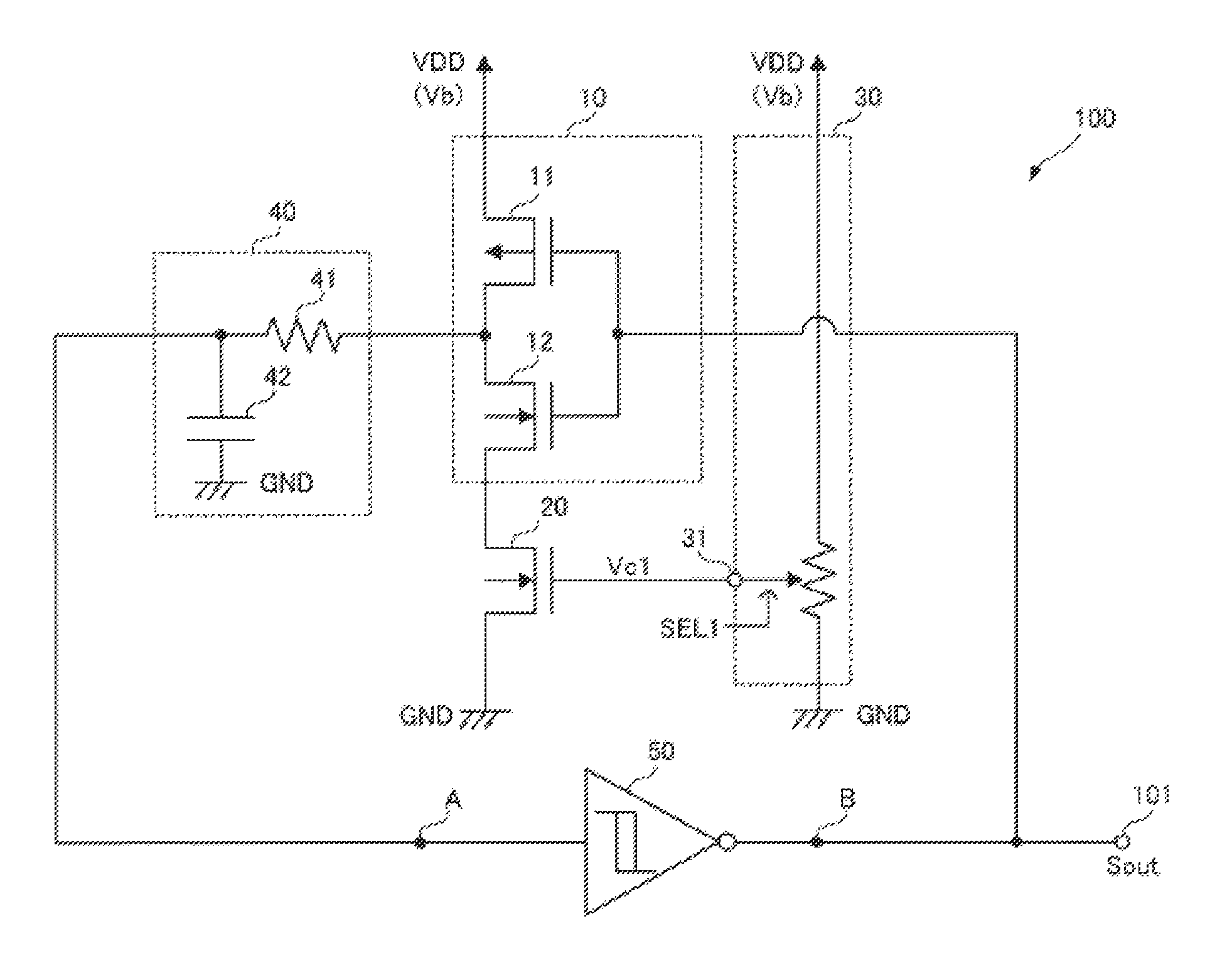
[0027]A first embodiment of the present invention will be explained. FIG. 1 is a circuit diagram showing a configuration of an oscillation circuit 100 according to the first embodiment of the present invention.

[0028]As shown in FIG. 1, the oscillation circuit 100 includes an inverter 10; an N-MOS transistor 20; a control voltage generating circuit 30; an RC circuit 40; and a Schmitt trigger circuit 50.

[0029]In the first embodiment, each component of the oscillation circuit 100 may be formed in one single semiconductor chip. It should be noted that the present invention is not limited to the structure, and each component of the oscillation circuit 100 may be formed in different semiconductor chips. Further, it should be noted that the RC circuit 40 may be formed of a discrete component.

[0030]In the first embodiment, the inverter 10 includes a P-MOS transistor 11 and an N-MOS transistor 12 connected in series. The P-MOS transistor 11 has a source connected to a power source line VDD; ...

second embodiment

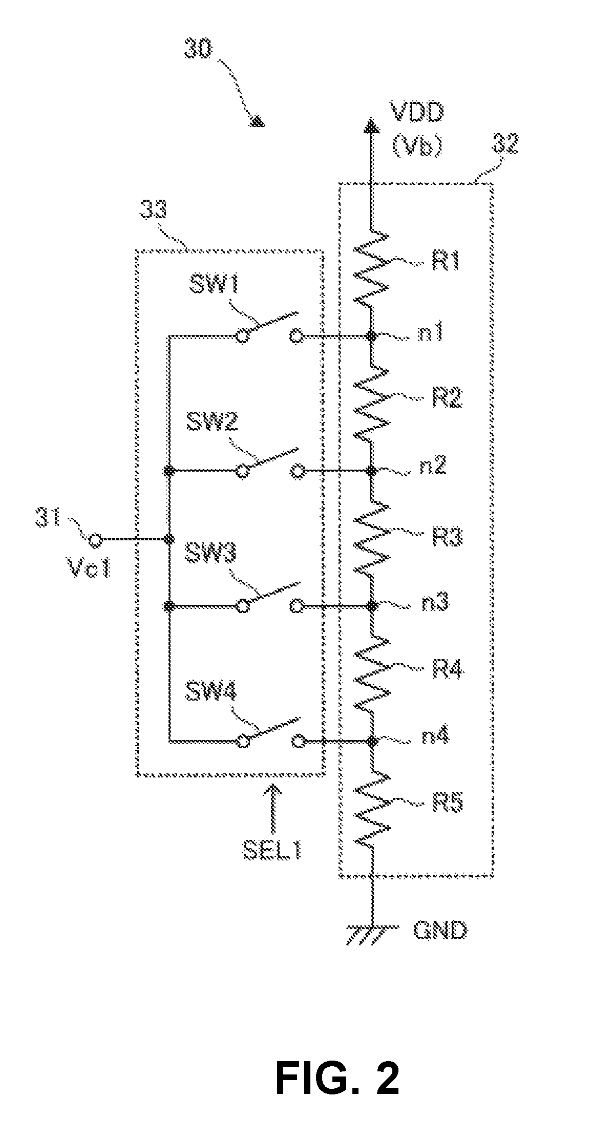
[0066]A second embodiment of the present invention will be explained next. FIG. 6 is a circuit diagram showing a configuration of an oscillation circuit 100A according to the second embodiment of the present invention.

[0067]As shown in FIG. 6, the oscillation circuit 100A includes a control voltage generating circuit 30A having a configuration different from that of the control voltage generating circuit 30 of the oscillation circuit 100 in the first embodiment.

[0068]In the second embodiment, similar to the control voltage generating circuit 30 in the first embodiment, the control voltage generating circuit 30A is configured to generate the control voltage Vc1 having the magnitude corresponding to the power source voltage Vb supplied between the power source line VDD and the ground line GND. Further, the control voltage generating circuit 30A is configured to output and supply the control voltage Vc1 to the gate of the N-MOS transistor 20 through the output terminal 31.

[0069]More sp...

third embodiment

[0078]A third embodiment of the present invention will be explained next. FIG. 8 is a circuit diagram showing a configuration of an oscillation circuit 100B according to the third embodiment of the present invention.

[0079]As shown in FIG. 8, the oscillation circuit 100B includes a selection signal generating portion 60 in addition to the configuration of the oscillation circuit 100A in the second embodiment.

[0080]In the third embodiment, the selection signal generating portion 60 is configured to generate the selection signal SEL1 and the selection signal SEL2 for setting the voltage division ratio of the control voltage generating circuit 30A. The selection signal generating portion 60 may be formed of, for example, a micro computer and a memory, so that the selection signal generating portion 60 executes a selection signal generating program stored in the memory to generate the selection signal SEL1 and the selection signal SEL2. It should be noted that the selection signal genera...


PUM


Abstract

An oscillation circuit includes an electrical current generating portion configured to generate an electrical current having an oscillation frequency decreasing as an amplitude thereof is decreased; a control voltage generating portion configured to generate a control voltage having a magnitude decreasing as a magnitude of a power source voltage is decreased; and an electrical current control portion. The electrical current control portion includes a first input terminal connected to the control voltage generating portion for receiving the electrical current; a control terminal connected to the control voltage generating portion for receiving the control voltage; and a first output terminal. The electrical current control portion is configured to reduce the amplitude of the electrical current flowing between the first input terminal and the first output terminal as the magnitude of the control voltage is decreased.

Description

BACKGROUND OF THE INVENTION AND RELATED ART STATEMENT[0001]The present invention relates to an oscillation circuit.[0002]A conventional oscillation circuit may include an inverter formed of a MOS (Metal Oxide Semiconductor) transistor.[0003]Patent Reference has disclosed an example of the conventional oscillation circuit. According to Patent Reference, the conventional oscillation circuit includes the inverter formed of a first P-channel MOS transistor and a first N-channel MOS transistor. Further, the conventional oscillation circuit includes a crystal oscillator connected between an input terminal and an output terminal of the inverter. Further, a second P-channel MOS transistor and a second N-channel MOS transistor are connected in series to a power source side and a ground side of the inverter, respectively.[0004]Patent Reference: Japanese Patent Publication No. 06-45830[0005]According to Patent Reference, the conventional oscillation circuit further includes a voltage adjusting...

Claims


Application Information

Patent Timeline
Patent Type & Authority Patents(United States)
IPC IPC(8): H03B5/04H03L1/00H03K3/0231H03K3/011H03B5/24
CPCH03B5/24H03B5/04H03K3/011H03K3/0231H03L1/00
Inventor YAGI, KATSUYOSHI
Owner LAPIS SEMICON CO LTD
Why Eureka
Try Eureka