Enhanced sensitivity ion sensing devices

Inactive Publication Date: 2017-01-10
NXP USA INC
View PDF21 Cites 11 Cited by
  • Summary
  • Abstract
  • Description
  • Claims
  • Application Information

AI Technical Summary

Problems solved by technology

But the sense plate is a significant contributor to the size of an ISFET device, and thus larger sense plate areas increase the size of the ISFET device.
In addition, during fabrication of a typical CMOS ISFET, once the gate dielectric is formed, it is susceptible to damage, particularly plasma-induced damage from fa

Method used


Image

  • Enhanced sensitivity ion sensing devices
  • Enhanced sensitivity ion sensing devices
  • Enhanced sensitivity ion sensing devices

Examples


Embodiment Construction

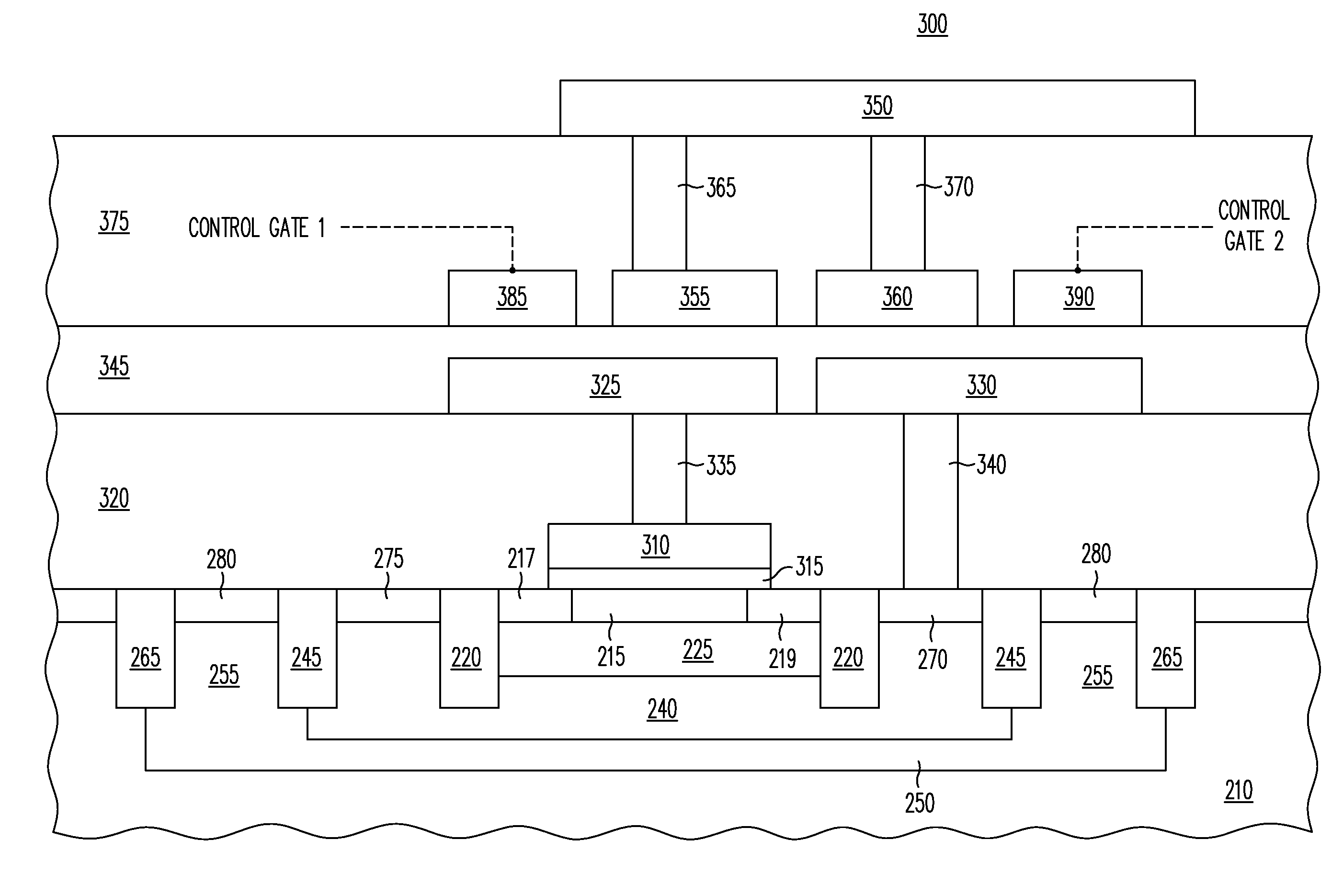
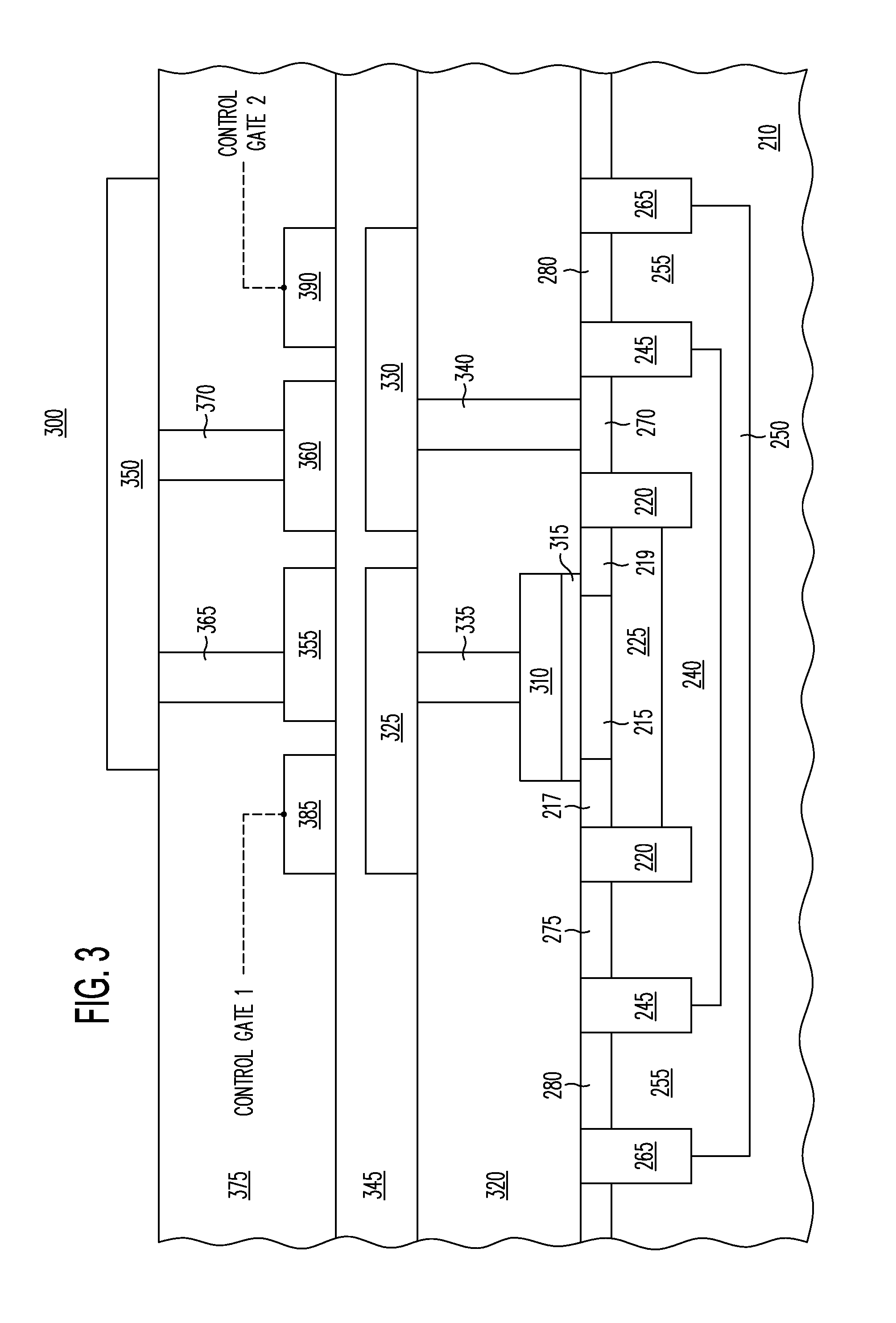
[0019]Embodiments of the present invention provide a mechanism for enhancing the sensitivity of an ion-sensitive semiconductor device (e.g., an ISFET) by creating a second gate coupled to the sense plate that can improve the amount of charge brought to the conductivity modulated region (e.g., transistor channel). This is accomplished by utilizing a buried dielectric layer associated with the ISFET channel region as the second transistor gate dielectric. The buried dielectric layer is coupled to the sense plate using an isolated well region as a conductor that is coupled to metal layers extending to the sense plate. Some embodiments further use the buried dielectric layer as the sole gate dielectric for the semiconductor device, thereby allowing the traditional gate dielectric region to be coupled to a protection diode. This protection diode then protects the gate dielectric from plasma induced damage and electrostatic discharge.

[0020]FIG. 1 is a simplified circuit representation of ...


PUM


Abstract

A mechanism is provided for enhancing the sensitivity of an ion-sensitive semiconductor device by creating a second gate coupled to a sense plate that can improve the amount of charge brought to the ion-sensitive semiconductor device conductivity modulated region (e.g., a channel region of an ISFET). This is accomplished by utilizing a buried dielectric layer associated with the ion-sensitive semiconductor device conductivity modulated region as the second gate dielectric. The buried dielectric layer is coupled to the sense plate using an isolated well region as a conductor that is coupled to metal layers extending to the sense plate. Some embodiments further use the buried dielectric layer as the sole gate dielectric for the semiconductor device, thereby allowing the traditional gate dielectric region to be coupled to a protection diode. This protection diode then protects the gate dielectric from plasma induced damage and electrostatic discharge.

Description

BACKGROUND[0001]Field[0002]This disclosure relates generally to ion sensing semiconductor devices, and more specifically, to a mechanism for enhancing sensitivity of ion sensing devices made using silicon on insulator techniques.[0003]Related Art[0004]Ion Sensitive Field Effect Transistors (ISFETs) are often used to sense a concentration of a target ion or molecule in an electrolytic solution. In early ISFET designs, the fluid being sensed was often in intimate contact with the gate dielectric, or separated from the gate dielectric by an ion-sensitive membrane. More current ISFET structures are made using CMOS process flows to create relatively low-cost devices with improved manufacturability. A typical CMOS ISFET includes a sense plate and a CMOS transistor, which includes a floating gate that is coupled to the sense plate. As is typical with a CMOS transistor, the gate is electrically isolated from the transistor channel through a gate dielectric.[0005]In order to measure the ioni...

Claims


Application Information

Patent Timeline
IPC IPC(8): G01N27/414G01N27/333
CPCG01N27/333G01N27/414G01N27/4145G01N27/4148
Inventor HOQUE, MD M.CHEN, WEIZEPARRIS, PATRICE M.
Owner NXP USA INC
Why Eureka
Try Eureka