Electrical analysis process

a technology of electrical analysis and analysis method, applied in the field of electrical design automation, can solve the problems of major reliability problems, degrade or destroy devices, etc., and achieve the effect of reducing the resistance only extraction

Active Publication Date: 2017-04-11
CADENCE DESIGN SYST INC
View PDF2 Cites 6 Cited by
  • Summary
  • Abstract
  • Description
  • Claims
  • Application Information

AI Technical Summary

Benefits of technology

[0004]In one or more embodiments of the present disclosure, a computer-implemented method for determining an effective electrical resistance in an electronic circuit design is provided. The method may include receiving, at one or more computing devices, an electronic circuit design and identifying one or more features associated with the electronic circuit design. The method may also include performing a resistance only extraction of a circuit net associated with the electroni...

Problems solved by technology

However, electrostatic discharge may alter the electrical characteristics of a semiconductor device, which may degrade or ...

Method used


Image

  • Electrical analysis process
  • Electrical analysis process
  • Electrical analysis process

Examples


Embodiment Construction

[0018]Reference will now be made in detail to the embodiments of the present disclosure, examples of which are illustrated in the accompanying drawings. The present disclosure may, however, be embodied in many different forms and should not be construed as being limited to the embodiments set forth herein. Rather, these embodiments are provided so that this disclosure will be thorough and complete, and will fully convey the concept of the disclosure to those skilled in the art.

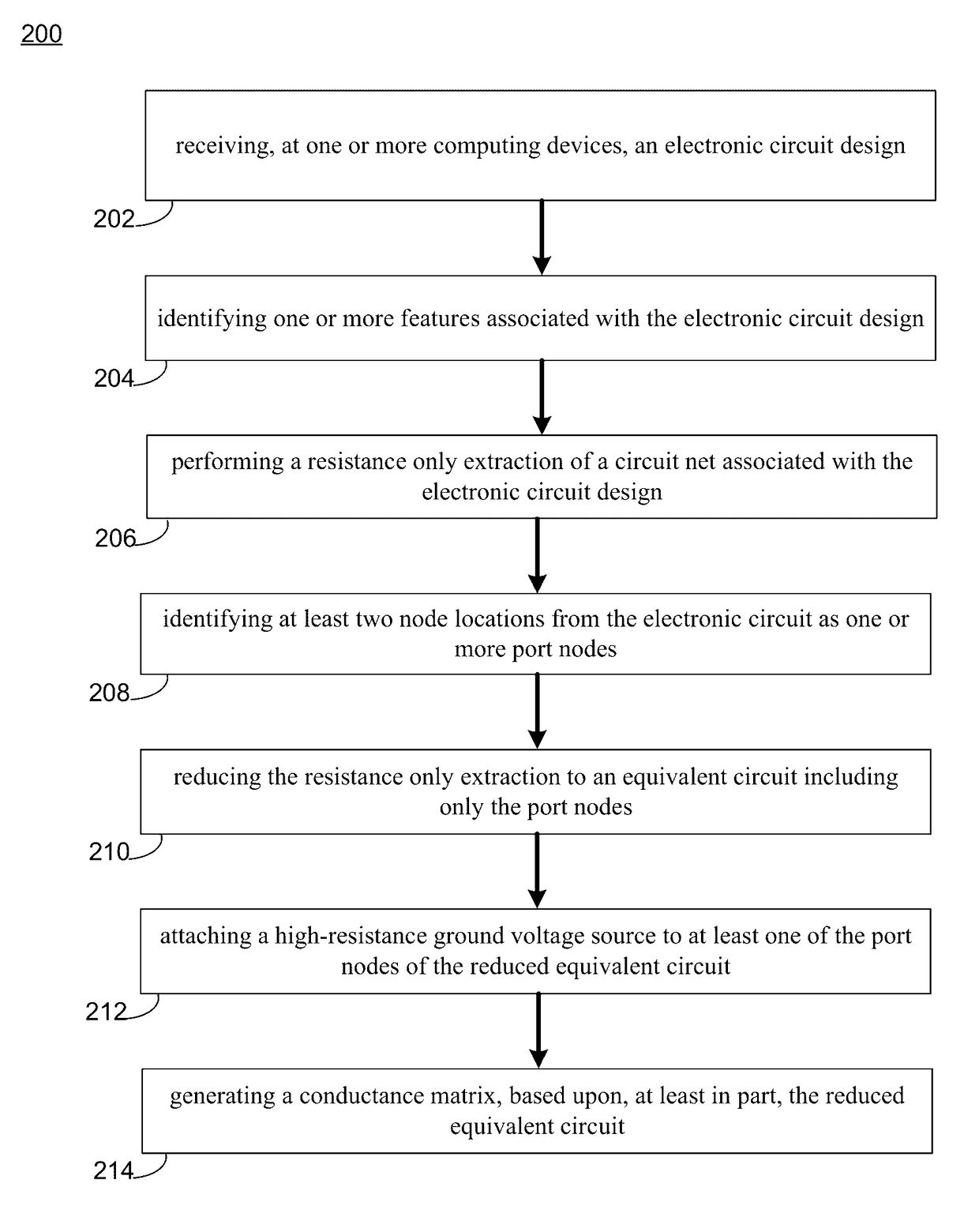
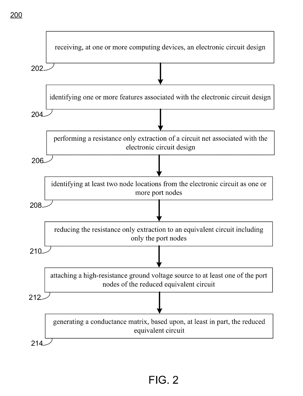
[0019]Embodiments of electrical analysis (“EA”) process 10 shown in FIGS. 1-5 may provide an efficient approach for computing the electrical equivalent impedance between all pairs of source and destination points for a given electrical circuit network. In other words, embodiments disclosed herein may be configured to compute the resistance from multiple sources to multiple destinations (N*M), ‘N’ times faster than existing techniques. Traditional approaches for solving this problem required placing a unit volt...


PUM


Abstract

The present disclosure relates to a system and method for determining an effective electrical resistance in an electronic circuit design. Embodiments may include receiving, at one or more computing devices, an electronic circuit design and identifying one or more features associated with the electronic circuit design. Embodiments may also include performing a resistance only extraction of a circuit net associated with the electronic circuit design and identifying at least two node locations from the electronic circuit as one or more port nodes. Embodiments may further include reducing the resistance only extraction to an equivalent circuit including only the port nodes and attaching a high-resistance ground voltage source to at least one of the port nodes of the reduced equivalent circuit. Embodiments may also include generating a conductance matrix, based upon, at least in part, the reduced equivalent circuit.

Description

FIELD OF THE INVENTION[0001]The present disclosure relates to electronic design automation (EDA), and more specifically, to a method for analyzing a model of an electrical circuit.DISCUSSION OF THE RELATED ART[0002]EDA utilizes software tools that may be used in the design and analysis of numerous electronic systems such as printed circuit boards (PCBs) and integrated circuits (ICs). Some EDA tools are configured to handle the issue of electro static discharge (“ESD”). ESD generally relates to the transfer of charge between bodies at different electrical potentials. However, electrostatic discharge may alter the electrical characteristics of a semiconductor device, which may degrade or destroy the device. As ESD is a high surge current event it has become a major reliability problem in the semiconductor industry.[0003]In order to protect the functional modules in integrated circuits from ESD events, protection cells are often utilized, generally between the functional modules and th...

Claims


Application Information

Patent Timeline
IPC IPC(8): G06F17/50
CPCG06F17/5068G06F30/398G06F30/367
Inventor RAI, NITYANANDGU, XINZHENG, HUI
Owner CADENCE DESIGN SYST INC
Why Eureka
Try Eureka