Array antenna

a technology of array antennas and antennas, applied in the field of array antennas, can solve the problems of increasing device size and complicated structure, and achieve the effect of reducing the size of array antennas and increasing the area utilization efficiency of substrates

Active Publication Date: 2017-07-04
MURATA MFG CO LTD
View PDF34 Cites 8 Cited by
  • Summary
  • Abstract
  • Description
  • Claims
  • Application Information

AI Technical Summary

Benefits of technology

[0009]The antennas disclosed in Patent Documents 1 and 2 exhibit low directivity toward an undersurface on which a ground layer is formed and have a narrow communication region. On the other hand, in the configuration disclosed in Patent Document 3 in which a plurality of antennas are oriented in different directions, a wide communication region is obtained. However, these antennas are independent of each other. A device therefore increases in size and has a complicated structure. In an antenna device disclosed in Patent Document 4 in which antennas are formed on both sides of a printed circuit board, ground layers are formed on both sides of the printed circuit board and radiation elements are disposed at the corresponding ground layers. The total thickness of the antenna device is the sum of the thickness of the printed circuit board and the thicknesses of the two antennas. The antenna device therefore increases in thickness and size.
[0012]According to the present disclosure, since a front-side antenna portion including a front-side radiation element disposed on or near the front side of a substrate and a back-side antenna portion including a back-side radiation element disposed on or near the back side of the substrate are provided, both sides of the substrate can have directivity and a communication region can be increased as compared with a case in which only one side of a substrate has directivity. The front-side radiation element in the front-side antenna portion and the back-side radiation element in the back-side antenna portion are disposed so as not to overlap each other when being vertically projected onto the back side of the substrate. Accordingly, the front-side ground layer in the front-side antenna portion can be formed on or near the back side of the substrate and the back-side ground layer in the back-side antenna portion can be formed on or near the front side of the substrate. In order to achieve wider frequency bands of the front-side antenna portion and the back-side antenna portion, it is therefore possible to obtain a large thickness dimension between a ground layer and a radiation element while reducing, or not increasing the thickness dimension of the substrate. As a result, a small-sized array antenna including a substrate having a small thickness dimension can be obtained.
[0014]According to the present disclosure, since the front-side ground layer faces the front-side radiation element, the front-side ground layer and the front-side radiation element can form a patch antenna. Since the back-side ground layer faces the back-side radiation element, the back-side ground layer and the back-side radiation element can form a patch antenna. Since the front-side ground layer is formed on or near the back side of the substrate and the back-side ground layer is formed on or near the front side of the substrate, it is possible to obtain a large thickness dimension between a ground layer and a radiation element while reducing the thickness dimension of the substrate. A patch antenna with a wide frequency band can be obtained. Furthermore, antenna space can be efficiently used and a small-sized array antenna can be obtained.
[0016]According to the present disclosure, since the conductor connection portion is disposed in the multilayer substrate to surround the front-side radiation element and the back-side radiation element, a wall can be provided between the front-side antenna portion and the back-side antenna portion by the conductor connection portion. It is therefore possible to suppress the mutual interference between the front-side antenna portion and the back-side antenna portion.
[0020]According to the present disclosure, when the front-side radiation element and the back-side radiation element are vertically projected onto the back side of the substrate, a gap between them is set to a predetermined value based on frequencies to be radiated. When the gap between the front-side radiation element and the back-side radiation element is small, mutual coupling between the front-side radiation element and the back-side radiation element becomes stronger and the characteristics of the array antenna are adversely affected. On the other hand, when the gap between the front-side radiation element and the back-side radiation element is large, the side lobe is increased and an antenna gain in a front direction is reduced. By setting the gap between the front-side radiation element and the back-side radiation element to a predetermined value, these problems can be avoided.
[0022]According to the present disclosure, when the front-side radiation elements and the back-side radiation elements are vertically projected onto the back side of the substrate, the front-side radiation elements are arranged in a staggered pattern and the back-side radiation elements are arranged in a staggered pattern. Accordingly, the area usage efficiency of the substrate is increased and the array antenna can be reduced in size.

Problems solved by technology

A device therefore increases in size and has a complicated structure.

Method used


Image

  • Array antenna
  • Array antenna
  • Array antenna

Examples


first embodiment

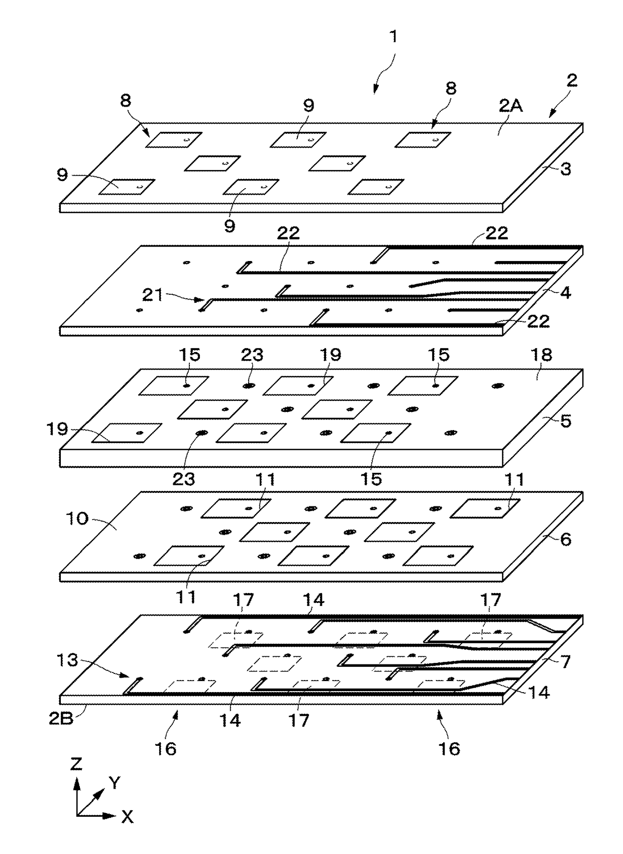
[0039]An array antenna 1 according to the present disclosure is illustrated in FIGS. 1 to 5. The array antenna 1 includes a multilayer substrate 2, a front-side antenna portion 8, and a back-side antenna portion 16.

[0040]The multilayer substrate 2 is formed in a flat shape parallel to the X-Y plane among the X-axis, Y-axis, and Z-axis directions that are mutually orthogonal. The multilayer substrate 2 has a dimension of several mm to several cm in the X-axis and Y-axis directions and a dimension of several hundred μm in the Z-axis direction that is the thickness direction.

[0041]The multilayer substrate 2 is a printed circuit board obtained by laminating five layers, for example, thin insulating resin layers 3 to 7, from a front side 2A to a back side 2B. As an example of the multilayer substrate 2, a resin substrate is used. However, the multilayer substrate 2 may be a ceramic multilayer substrate obtained by laminating insulating ceramic layers or a low temperature co-fired ceramic...

second embodiment

[0076]In the second embodiment, the front-side radiation elements 33 and the back-side ground layer 18 are formed on the same layer and the back-side radiation elements 37 and the front-side ground layer 10 are formed on the same layer. However, a radiation element and a ground layer may be on different layers.

[0077]In the array antennas 1 according to the first embodiment and the array antenna 31 according to the second embodiment, a plurality of strip lines, the strip lines 14 and the strip lines 22, are formed. If there is no need to scan a radiation beam in the X-axis direction and the Y-axis direction, a common signal may be supplied to the front-side radiation elements 9 via a strip line 42 having an end portion divided into branches and a common signal may be supplied to the back-side radiation elements 17 via a strip line 43 having an end portion divided into branches like in, for example, an array antenna 41 that is the first modification illustrated in FIG. 10. This config...

third embodiment

[0085]A conductor connection portion is formed with the vias 52 in the third embodiment, but may be formed with, for example, a conductor film. This configuration can be applied to the second modification.

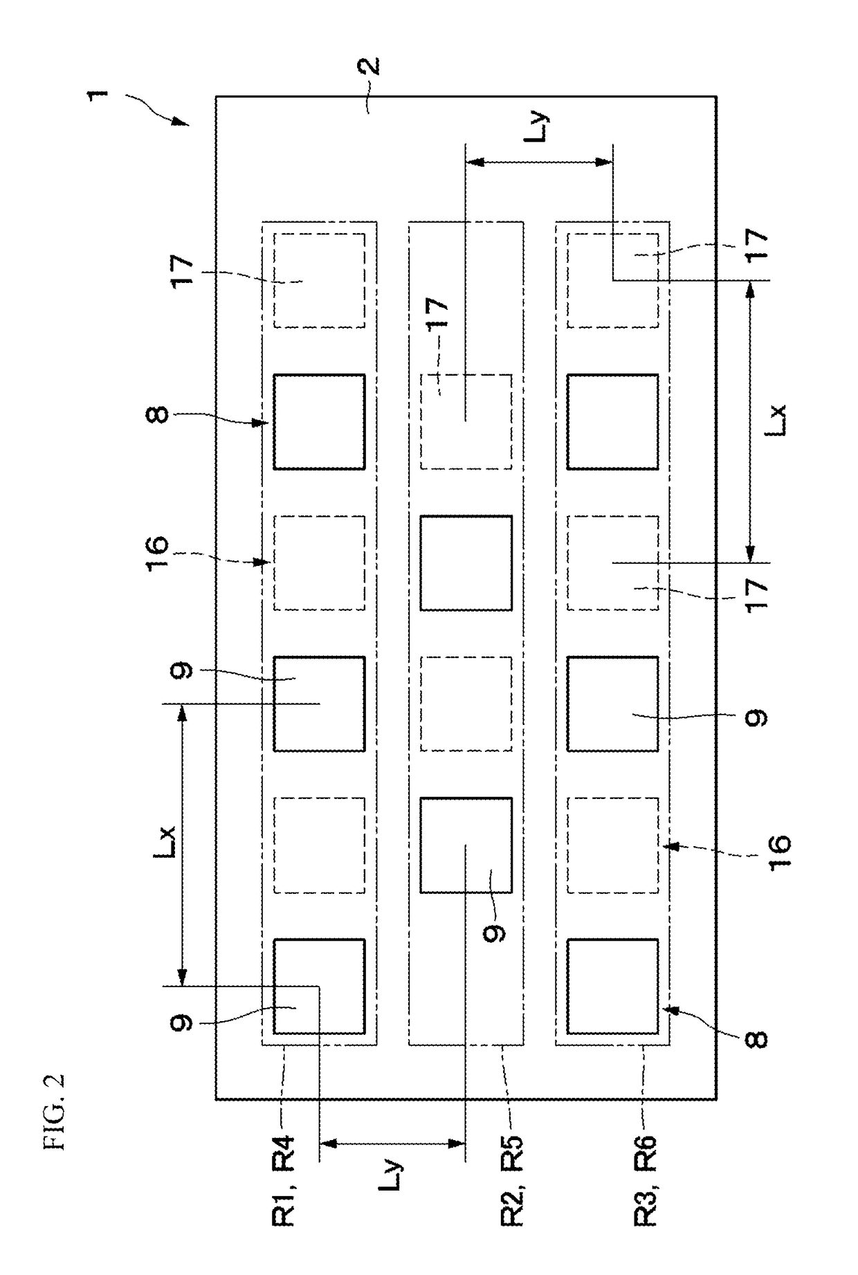
[0086]In the above-described embodiments, an array antenna (1, 31, and 51) includes eight front-side antenna portions (8 and 32) and eight back-side antenna portions (16 and 36). The numbers of the front-side antenna portions and the back-side antenna portions may be one, in the range of two to seven, or nine or more. The numbers of the front-side antenna portions and the back-side antenna portions do not necessarily have to be the same and may be different. This configuration can also be applied to the first and second modifications.

[0087]The front-side antenna portions 8 and 32 and the back-side antenna portions 16 and 36 are disposed on a plane extending in the X-axis direction and the Y-axis direction in the above-described embodiments, but may be arranged in a straight line. T...


PUM


Abstract

In a multilayer substrate, eight front-side antenna portions and eight back-side antenna portions are disposed. Front-side radiation elements in the front-side antenna portions and back-side radiation elements in the back-side antenna portions are arranged in a staggered pattern when being vertically projected onto an back side of the multilayer substrate. The front-side radiation elements are disposed on a front side of the multilayer substrate, and a front-side ground layer is formed near the back side of the multilayer substrate. On the other hand, the back-side radiation elements are disposed on the back side of the multilayer substrate, and a back-side ground layer is formed near the front side of the multilayer substrate. The front-side radiation element and the back-side radiation element are disposed so as not to overlap each other when being vertically projected onto the back side of the multilayer substrate.

Description

BACKGROUND OF THE INVENTION[0001]Field of the Invention[0002]The present disclosure relates to an array antenna including a plurality of antennas formed in a substrate.[0003]Description of the Related Art[0004]Patent Document 1 discloses a microstrip antenna (patch antenna) including a radiation element and a ground layer which face each other across a dielectric having a small thickness relative to a wavelength and a passive element disposed on the radiation surface side of the radiation element. Patent Document 2 discloses an array antenna in which a plurality of antennas are connected by a plurality of transmission lines. Patent Document 3 discloses a configuration in which two or more disc-shaped antennas are coupled in parallel and have directivities in different directions. Patent Document 4 discloses a configuration in which antennas are formed on either side of a substrate.[0005]Patent Document 1: Japanese Unexamined Patent Application Publication No. 55-93305[0006]Patent Do...

Claims


Application Information

Patent Timeline
Patent Type & Authority Patents(United States)
IPC IPC(8): H01Q9/42H01Q21/06
CPCH01Q9/42H01Q21/06H01Q9/0414H01Q21/0006H01Q21/065H01Q21/28H01Q9/0407H01Q25/005
Inventor SUDO, KAORUNAKAJIMA, MASAYUKI
Owner MURATA MFG CO LTD
Why Eureka
Try Eureka