Bonding apparatus

a technology of bonding apparatus and electrode pads, which is applied in the direction of soldering apparatus, auxillary welding devices, manufacturing tools, etc., can solve the problems of time and effort in process margins (setting conditions), and the like, so as to prevent the failure of bonding between the device chips and electrode pads, the effect of finding optimal bonding conditions

Inactive Publication Date: 2017-07-18
TORAY ENG CO LTD
View PDF41 Cites 6 Cited by
  • Summary
  • Abstract
  • Description
  • Claims
  • Application Information

AI Technical Summary

Benefits of technology

[0008]When a plurality of device chips are bonded on a substrate constituting a substrate module, bonding the device chips all at once is preferable to bonding them one by one in terms of improving productivity. Conductive pastes used for bonding (hereinafter referred to as bonding pastes) that are applied to bond electrode pads and device chips are only applied in the smallest amount required, while still affording good bonding, in order to prevent short-circuiting between adjacent electrodes or device chips.
[0011]In view of this, it is an object of the present application to provide a bonding apparatus with which bonding failures between device chips and electrode pads can be prevented in the simultaneous bonding of a plurality of device chips, and the optimal bonding conditions can be found quickly.
[0052]In the simultaneous bonding of a plurality of device chips, bonding failure between the device chips and electrode pads can be prevented, and the optimal bonding conditions can be found quickly.

Problems solved by technology

However, the work entailed by finding these optimal bonding conditions and process margins (setting the conditions) takes time and effort because it involves finding by trial and error the bonding conditions at which bonding failure will not occur, while confirming the bonding strength of the various device chips.

Method used


Image

  • Bonding apparatus
  • Bonding apparatus
  • Bonding apparatus

Examples


Embodiment Construction

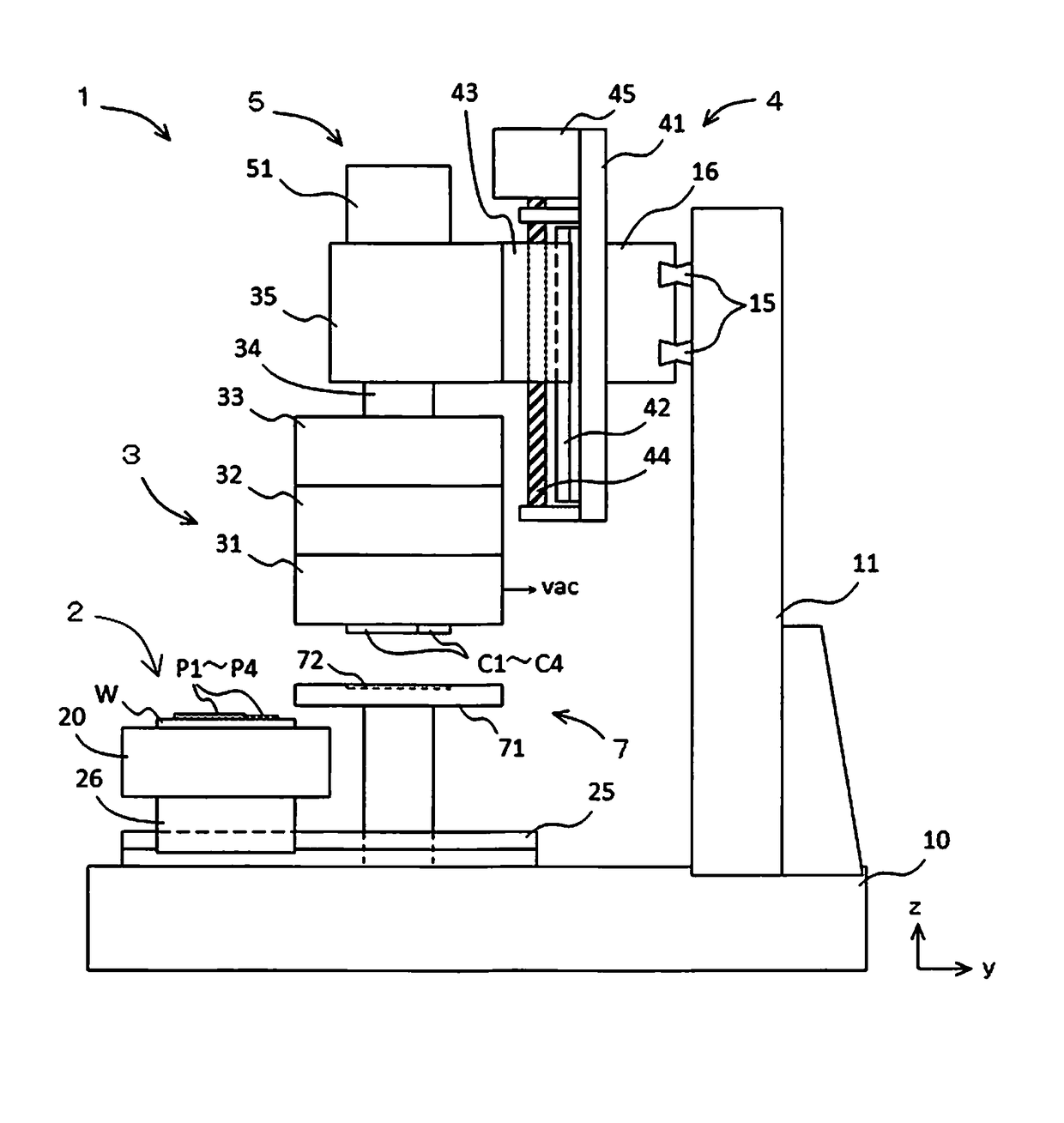
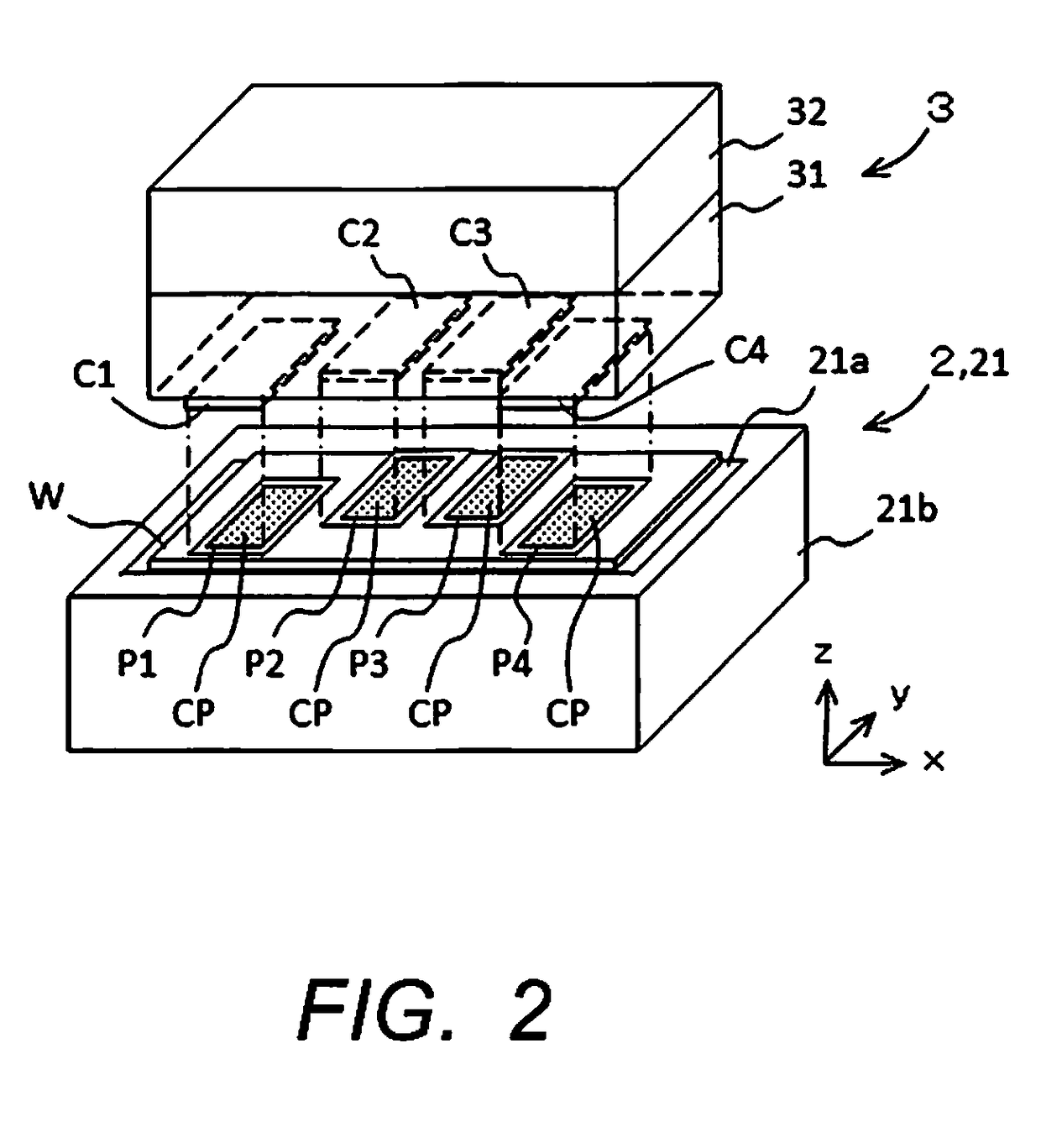
[0062]An embodiment of the present invention will now be described through reference to the drawings. To simplify the description, an example will be given in which four electrode pads P1 to P4 are formed on the surface of a substrate W (the bonding object), and device chips C1 to C4 are bonded over these.

[0063]In the drawings, the three axes of a rectangular coordinate system are labeled X, Y, and Z, the XY plane is the horizontal plane, and the Z direction is the vertical direction. In particular, the X direction is shown such that the arrow direction represents the side closer to the viewer and the opposite direction the side farther away from the viewer. For the Y direction, the arrow direction is to the right side, and the opposite direction to the left side. For the Z direction, the arrow direction (gravitationally upward) is the upper side, and the opposite direction the lower side.

[0064]FIG. 1 is a simplified overall diagram of a specific embodiment of the present invention....


PUM

PropertyMeasurementUnit
bulge distancesaaaaaaaaaa
transparentaaaaaaaaaa

Abstract

A bonding apparatus bonds a plurality of device chips on a plurality of electrode pads that are provided to a surface of a substrate. The bonding apparatus includes a stage, a head unit, a head lifting mechanism, a head vibrator, a heater, and a bonding region observation component. The substrate is placed and supported on the stage. The head unit holds the device chips. The head lifting mechanism raises and lowers the head unit in an up and down direction relative to the stage. The head vibrator vibrate the head unit in the up and down direction. The heater heats a bonding paste that bonds the device chips and the electrode pads. The bonding region observation component observes a region that includes at least a peripheral part of the electrode pads.

Description

CROSS-REFERENCE TO RELATED APPLICATIONS[0001]This application is a U.S. National stage of International Application No. PCT / JP2014 / 078542 filed on Oct. 28, 2014. This application claims priority to Japanese Patent Application No. 2013-231148 filed with Japan Patent Office on Nov. 7, 2013. The entire disclosure of Japanese Patent Application No. 2013-231148 is hereby incorporated herein by reference.BACKGROUND[0002]Field of the Invention[0003]The present invention relates to a bonding apparatus for bonding device chips onto a substrate coated with a bonding paste over electrode pads.[0004]Background Information[0005]Substrate modules in which parts (known as device chips) containing resistors, capacitors, reactance elements, switching circuits, or the like are bonded on a wiring board have been used in the past in a variety of applications.[0006]As hybrid automobiles and electric automobiles have gained in popularity in recent years, substrate modules in which device chips called pow...

Claims


Application Information

Patent Timeline
Patent Type & Authority Patents(United States)
IPC IPC(8): B23K37/00B23K3/04B23K1/06B23K1/00H05K3/00H01L23/00B23K3/08B23K3/06B23K37/04H05K3/34
CPCH01L24/75B23K1/0016B23K1/06B23K3/04B23K3/0638B23K3/08B23K37/04H01L24/83H01L24/95H05K3/0008H01L24/27H01L24/29H01L24/32H01L2224/2732H01L2224/29298H01L2224/29339H01L2224/32225H01L2224/753H01L2224/7598H01L2224/75301H01L2224/75745H01L2224/75824H01L2224/75901H01L2224/8384H01L2224/83192H01L2224/83908H05K3/3436H05K2203/163H05K2203/166
Inventor WADA, HIROMITSU
Owner TORAY ENG CO LTD
Why Eureka
Try Eureka